

Optical device and method of controlling the same
A technology of optical devices and optical components, applied in the field of optical devices and controlling the optical devices
- Summary
- Abstract
- Description
- Claims
- Application Information
AI Technical Summary
Problems solved by technology
Method used
Image

Examples
no. 1 approach
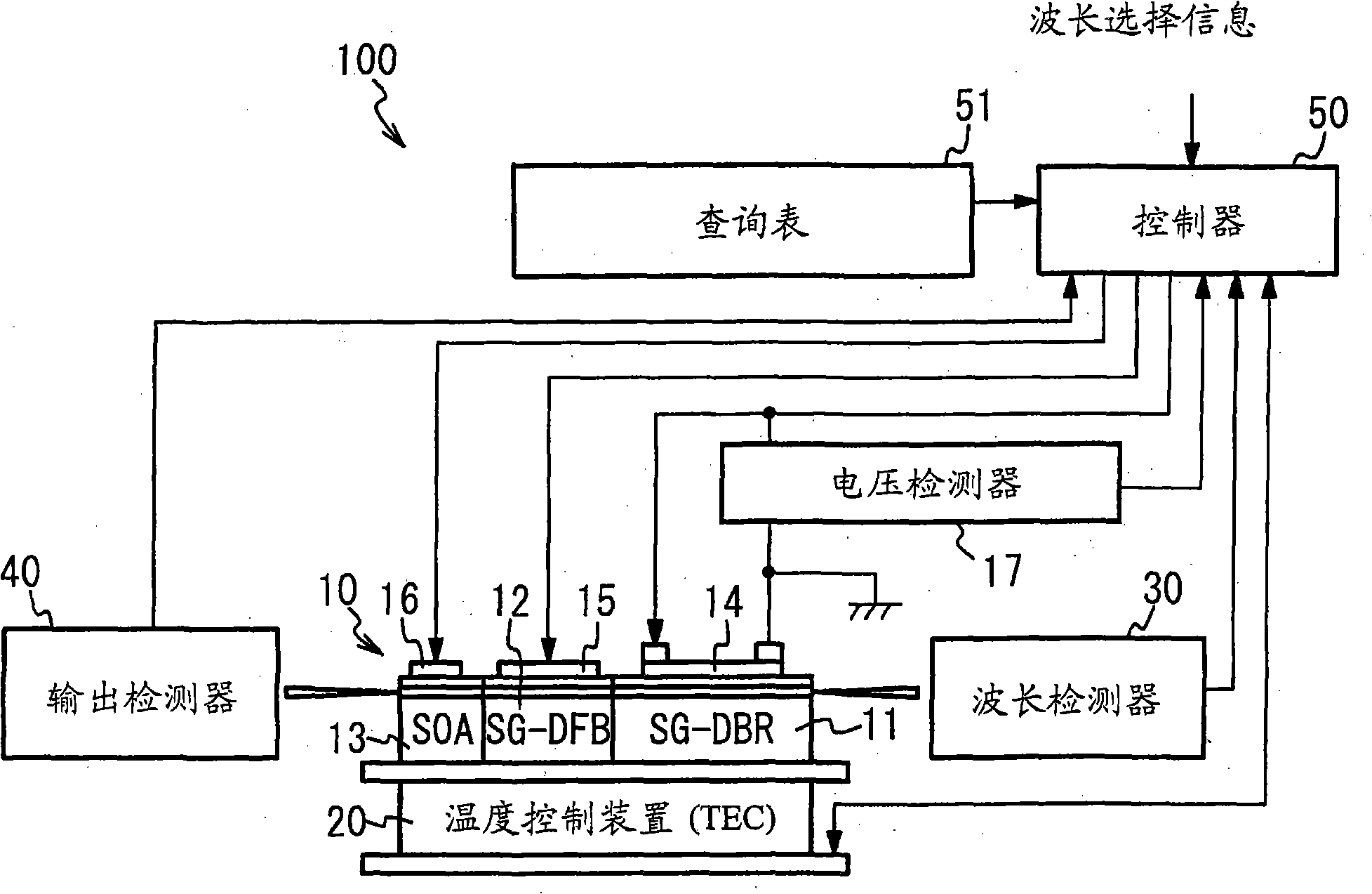
[0025] Next, a semiconductor laser as an optical element will be described. figure 1 The structures of the semiconductor laser 10 and the laser device 100 having the semiconductor laser 10 according to the first embodiment are illustrated. Such as figure 1 As shown, the laser device 100 has: a semiconductor laser 10 , a temperature control device 20 , a wavelength detector 30 , an output detector 40 and a controller 50 . The semiconductor laser 10 is mounted on a temperature control device 20 . Each component is described below.
[0026] The semiconductor laser 10 has a structure in which an SG-DBR region 11 , an SG-DFB region 12 , and a semiconductor amplifier (SOA: Semiconductor Optical Amplifier) region 13 are sequentially coupled. The SG-DBR region 11 has optical waveguides in which gratings are provided at predetermined intervals. That is, the optical waveguide of the SG-DBR region 11 has a first region having a diffraction grating, and a second region optically con...
no. 2 approach
[0049] In the second embodiment, a semiconductor laser having the aforementioned CSG-DBR will be described. Figure 5 The structures of the semiconductor laser 10a and the laser device 100a having the semiconductor laser 10a are illustrated. Such as Figure 5 As shown, the semiconductor laser 10 a has a CSG-DBR region 11 a instead of the SG-DBR region 11 . In this embodiment, the CSG-DBR region 11a has three segments with a combination of gratings and spacers. Therefore, for each segment, three heaters 14a, 14b, and 14c are provided on the CSG-DBR region 11a. And for each heater, voltage detectors 17a, 17b, and 17c are provided.
[0050] In this embodiment, while the electric power supplied to each heater is feedback-controlled to be kept constant based on the detection result of each voltage detector, the calorific value of each heater can be kept constant. Therefore, the semiconductor laser 10a acquires a desired oscillation wavelength.
[0051] The number of gratings a...
no. 3 approach
[0053] The present invention can be applied to other optical elements than semiconductor lasers. For example, the invention can be applied to mach-Zehnder optical switches. Such optical switches are used in switching systems such as optical cross-connects.
[0054] Figure 6 The structure of the optical switch 200 according to the third embodiment is illustrated. Such as Figure 6 As shown, the optical switch 200 is made of a material having a thermo-optic effect such as a silicon-based material. The optical switch 200 has a mach-Zehnder interference structure having a first waveguide 201 and a second waveguide 202 . The optical switch 200 is provided on the temperature control device 210 . Thus, the temperature control device 210 controls the temperature of its various components.
[0055] The optical switch 200 has a heater 203 . The heater 203 heats the second waveguide 202 . This results in a change in the phase difference between the light propagating in the first...
PUM
 Abstract
Description
Claims
Application Information