

Ceramic moulding body, ceramic component, and manufacturing method of ceramic moulding body and ceramic component
A molded body and ceramic technology, which is applied in the direction of electrical components, printed circuit manufacturing, printed circuits, etc., can solve the problem of multi-layering of unsuitable conductor patterns, and achieve the effect of thickening thickness and easy impedance value
- Summary
- Abstract
- Description
- Claims
- Application Information
AI Technical Summary
Problems solved by technology
Method used
Image

Examples
no. 1 Embodiment approach
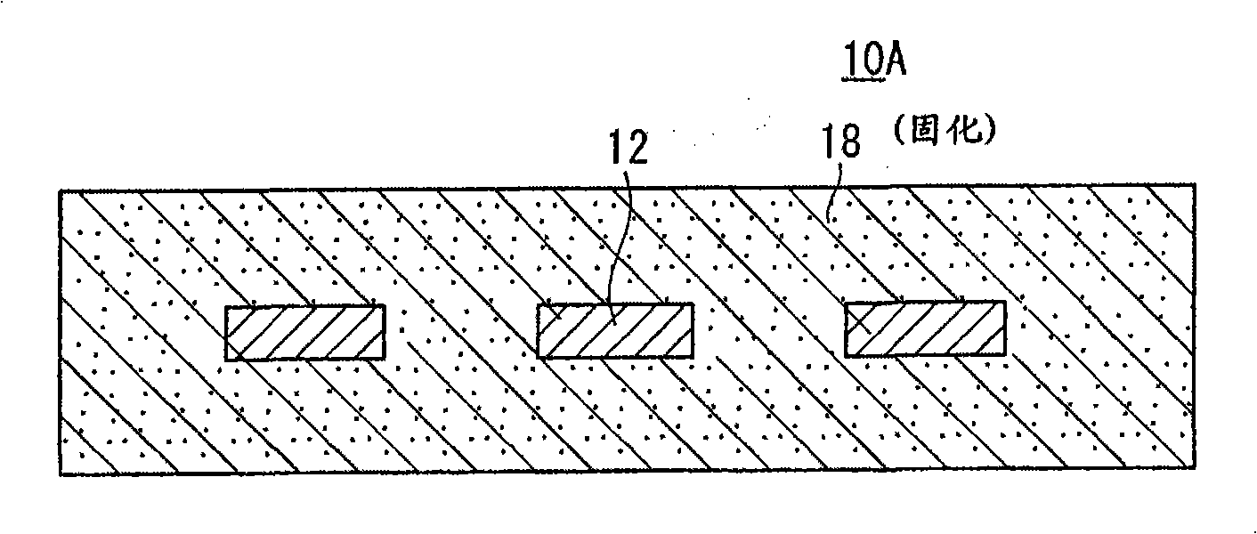
[0062] First, the ceramic molded body (hereinafter referred to as the first ceramic molded body 10A) according to the first embodiment is as follows: figure 1 As shown, it is constituted by embedding the conductor molded body 12 .
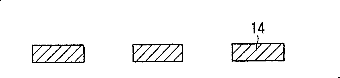
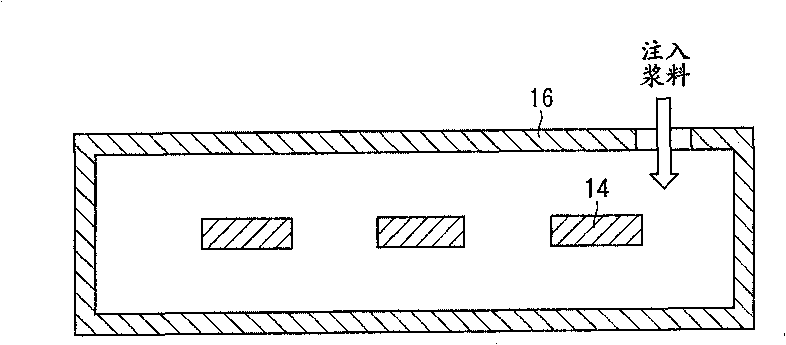
[0063] The first ceramic molded body 10A, such as Figure 2A As shown, the conductive paste 14 containing resin and powder of at least one metal of silver (Ag), gold (Au), and copper (Cu) is molded and solidified into a predetermined shape, and then, as shown in FIG. Figure 2B As shown, it is set in the casting mold 16, and the ceramic colloid molding slurry (hereinafter referred to as slurry 18) containing a thermosetting resin precursor, ceramic powder and solvent is poured into the casting mold 16, and then solidified to obtain (refer to Figure 2C ) The ceramic molded body. Here, even if a part of the structure of the casting mold 16 is opened as shown in the cross section, there is no problem as long as there is no leakage of the slurry 18 ...
no. 2 Embodiment approach
[0145] Next, for the ceramic molded body (hereinafter referred to as the second ceramic molded body 10B) according to the second embodiment, refer to Figure 11 to Figure 15 Be explained.
[0146] The second ceramic molded body 10B, such as Figure 11 As shown, it is obtained by applying a slurry 18 mixed with a thermosetting resin precursor, ceramic powder, and a solvent, coating the conductor molded body 12, and then curing it. When the thickness of the second ceramic molded body 10B is as thin as 0.05 mm or less, it is difficult to adopt a method of casting into a mold, so a method of coating onto a substrate is preferable.
[0147] Here, specifically, for the manufacturing method of the second ceramic molded body 10B and the second ceramic component, refer to Figure 12A ~ Figure 14C to explain.
[0148] First, if Figure 12A As shown, a release agent (not shown) is applied on the upper surface of the substrate 64 such as a film, and then, for example, the conductive p...
no. 3 Embodiment approach
[0182] It has substantially the same configuration as the first ceramic molded body 10A or the second ceramic molded body 10B described above, but the composition of the slurry 18 is partially different.
[0183] That is, polybasic acid esters having two or more ester groups are used as the dispersion medium. In addition, as a thermosetting resin precursor, a gelling agent having an isocyanate group or an isothiocyanate group, and a polymer having a hydroxyl group or a molecule having a hydroxyl group are used. Further, a small amount of water may be added.
[0184] The isocyanate group reacts with water to form amine and carbon dioxide through carbamic acid, and the amine further reacts with another isocyanate group to form a urea group, and further, another isocyanate group reacts with a urea group to cross-link to form a biuret. When water is added, carbon dioxide (gas) is generated, so when the slurry 18 is solidified as it is, the gas remains as pores. Therefore, after m...
PUM
 Abstract
Description
Claims
Application Information