CMOS low-power consumption, low offset voltage, low return-stroke noise comparator

A technology with offset voltage and low power consumption, which is applied in the field of wireless communication systems, can solve the problems of complex control clock phase, difficulty in obtaining conversion speed, and increased clock cost, so as to optimize the design of transistor size, eliminate slew rate restrictions, reduce The effect of small overdrive recovery time

Inactive Publication Date: 2009-01-28
杭州中科微电子有限公司
View PDF0 Cites 28 Cited by
  • Summary
  • Abstract
  • Description
  • Claims
  • Application Information

AI Technical Summary

Problems solved by technology

H.Fiedler, et al., "A 5-bitbuilding block for 20MHz A/D converters," IEEE J.of Solid-State Circuits, vol.16, proposed a typical static latch comparator as figure 1 As shown, although the backhaul noise is low, there are obvious disadvantages: ① There are two DC paths from the power supply to the ground, and the power consumption is relatively large; rate limitation and low working speed; ③Using NMOS transistors as input differential pairs and diode-connected PMOS transistors as load c

Method used


Image

  • CMOS low-power consumption, low offset voltage, low return-stroke noise comparator
  • CMOS low-power consumption, low offset voltage, low return-stroke noise comparator
  • CMOS low-power consumption, low offset voltage, low return-stroke noise comparator

Examples


Embodiment Construction

[0033] The technical solutions of the present invention will be further described below in conjunction with the accompanying drawings and specific embodiments.

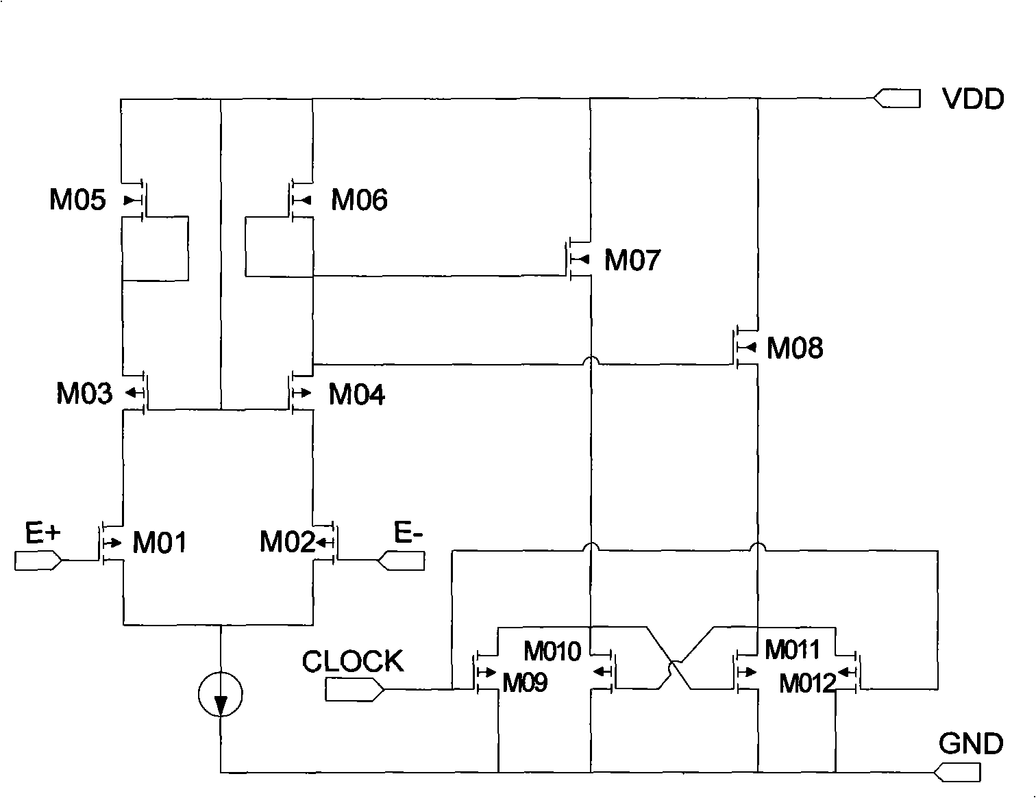
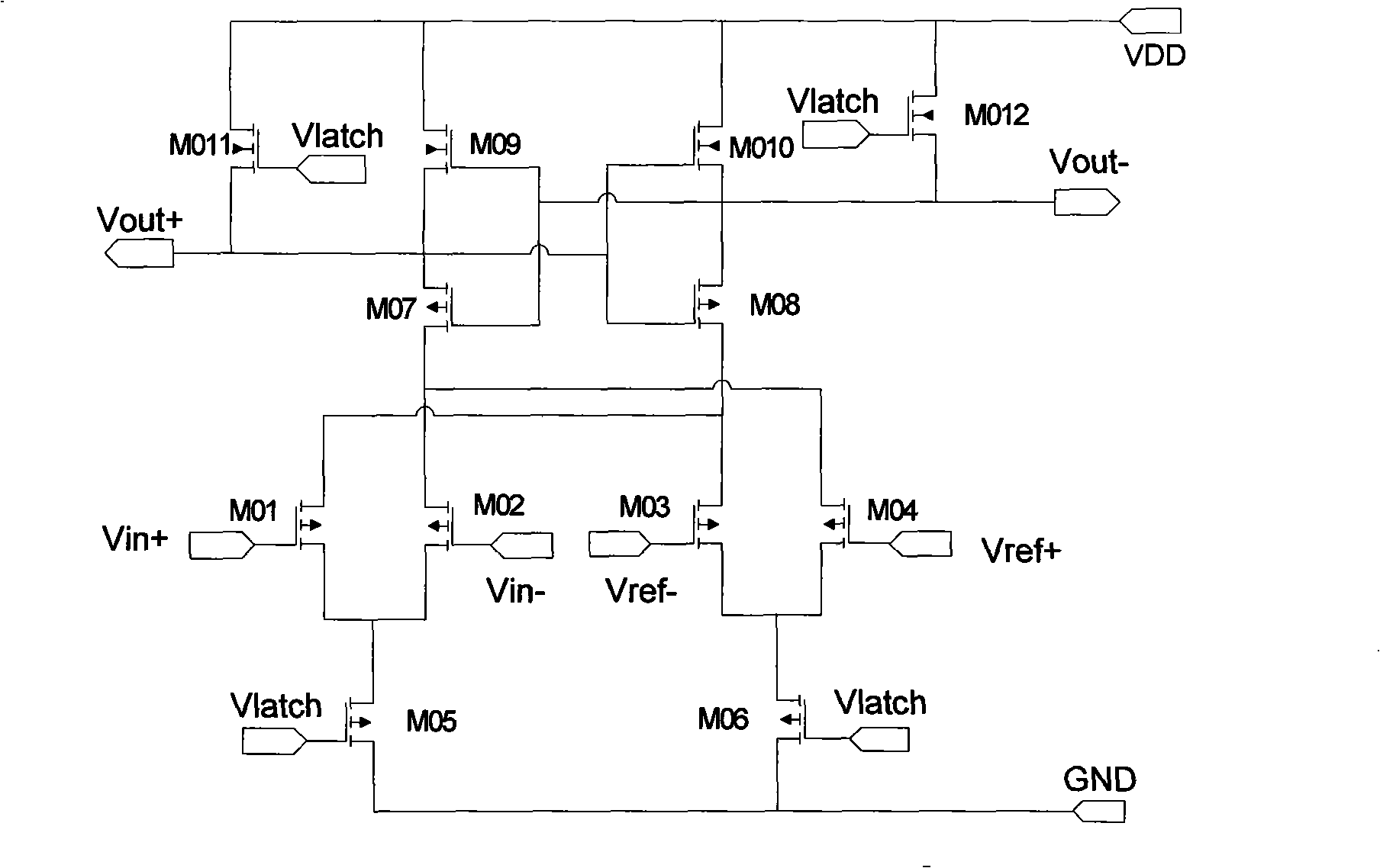
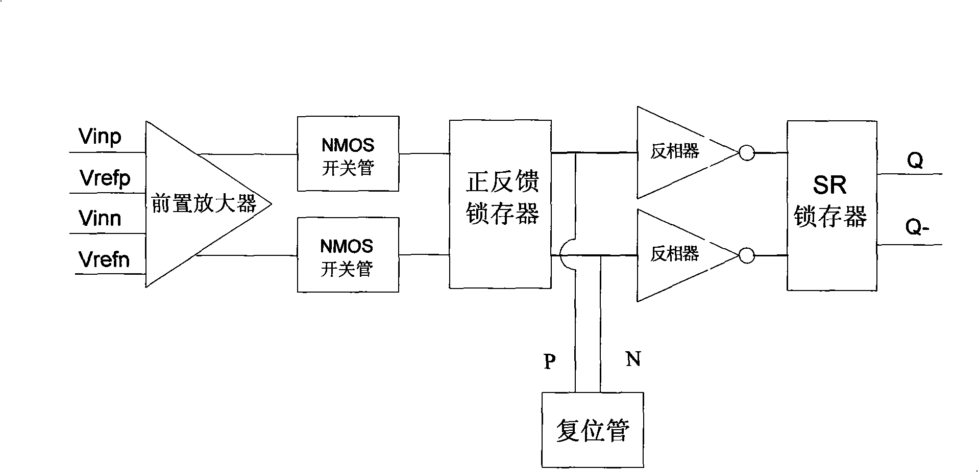
[0034] The principle block diagram of the CMOS low power consumption, low offset voltage, low backhaul noise comparator of the present invention is as image 3As shown, it includes a preamplifier, a pair of NMOS switches, a positive feedback latch, two CMOS inverters and an SR latch. The preamplifier uses PMOS double differential pair tubes as the input differential pair, a pair of diode-connected NMOS tubes and a pair of positive feedback connected NMOS tubes are connected in parallel as the active load circuit structure, and the input end of the PMOS double differential pair tubes Connect Vinp and Vinn terminals, Vrefp and Vrefn terminals respectively, connect a pair of NMOS switch tubes between the preamplifier and the positive feedback latch, connect a reset tube between the two output regeneration nodes P and N o...


PUM


Abstract

The invention discloses a CMOS comparator with low power consumption, low offset voltage and low return noise, belonging to the technical field of the radio communication system. The CMOS comparator comprises a preposing amplifier, a pair of switch tubes, a positive feedback latch unit, a CMOS phase inverter and an SR latch unit, wherein the preposing amplifier adopts a PMOS tube to serve as the input differential pairs, a diode is connected with an NMOS tube and is connected with a circuit structure which is in positive feedback connection with the NMOS tube in parallel to serve as the load so as to reduce the offset voltage of the comparator; the pair of the switch tubes is inserted between the preposing amplifier and the positive feedback latch unit so as to reduce the return noise of the comparator; and the positive feedback latch unit adopts a cross-coupling CMOS inverter circuit structure, a reset pipe is connected between regenerating nodes, thereby not only reducing the power consumption but also increasing the regenerating speed. The comparator has good properties of low power consumption, low offset voltage and low return noise, does not need to adopt the offset canceling technique, and can be widely applied to a low power consumption high-speed AD converter with 6 to 8 medium and high accuracy of a radio communication system.

Description

technical field [0001] The invention belongs to the technical field of wireless communication systems, and in particular relates to a CMOS voltage comparator, which is applied to a comparator with low power consumption, low offset voltage and low backhaul noise for analog-to-digital converters of portable equipment. Background technique [0002] In the front-end receivers of many contemporary wireless communication systems, high-speed, high-resolution analog-to-digital converters are required. For battery-powered portable device applications, the analog-to-digital converters are very demanding on power consumption. The wireless communication industries of various countries are committed to Research and design of high-speed, high-resolution, low-power analog-to-digital converters. As we all know, the comparator is the core circuit module of all analog-to-digital converters, and its characteristics such as offset voltage, power consumption, return noise, and comparison speed w...

Claims


Application Information

Patent Timeline
IPC IPC(8): H03K5/24H03M1/34
CPCY02B60/50
Inventor 莫太山马成炎叶甜春
Owner 杭州中科微电子有限公司
Why Eureka
Try Eureka