Wired circuit board and producing method thereof

A technology for wiring circuit substrates and coating layers, which is applied in the manufacture of printed circuits, printed circuits, printed circuit components, etc., can solve problems such as short circuit of conductor patterns, prevent ion migration, prevent discoloration, improve connectivity and connection durability Effect

Inactive Publication Date: 2009-01-28
NITTO DENKO CORP
View PDF1 Cites 1 Cited by
  • Summary
  • Abstract
  • Description
  • Claims
  • Application Information

AI Technical Summary

Problems solved by technology

[0003] In such a wired circuit board, if electricity is applied for a long period of time under high temperature and high humidity, ion migration occurs in which the copper of the conductive pattern moves to the insulating covering layer, and a short circuit may occur between the conductive patterns.

Method used


Image

  • Wired circuit board and producing method thereof
  • Wired circuit board and producing method thereof
  • Wired circuit board and producing method thereof

Examples


Embodiment 1

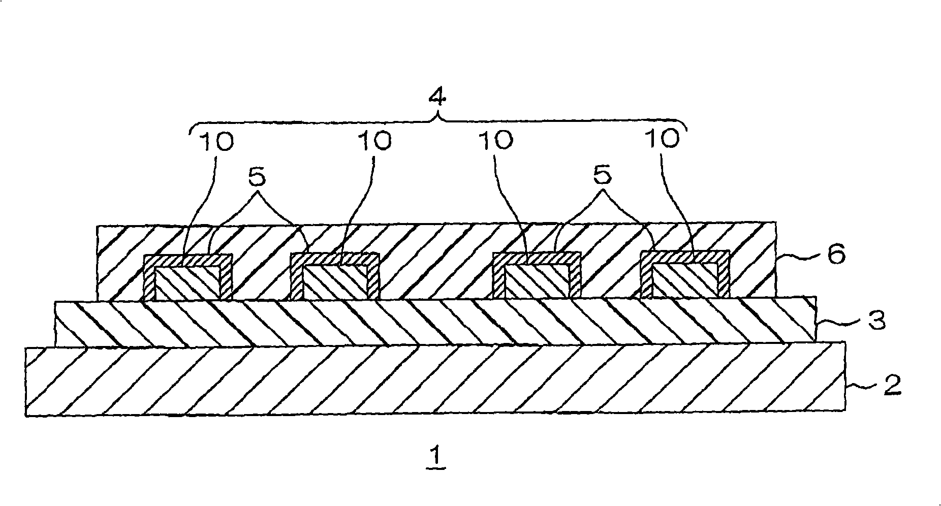
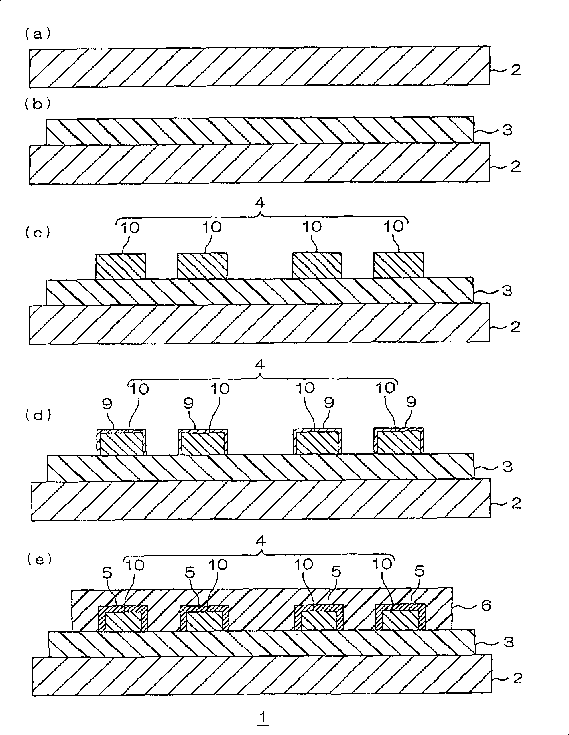
[0065] First, prepare a metal support substrate made of stainless steel with a thickness of 25 μm (see image 3 (a)) Furthermore, the varnish of the photosensitive polyamic-acid resin was apply|coated to the whole surface of a metal supporting board|substrate, and it heated at 90 degreeC for 15 minutes, and it dried. Then, after exposure and development, it was cured (imidized) by heating at 370° C. for 120 minutes under reduced pressure to form an insulating base layer with a thickness of 10 μm (see image 3 (b)).

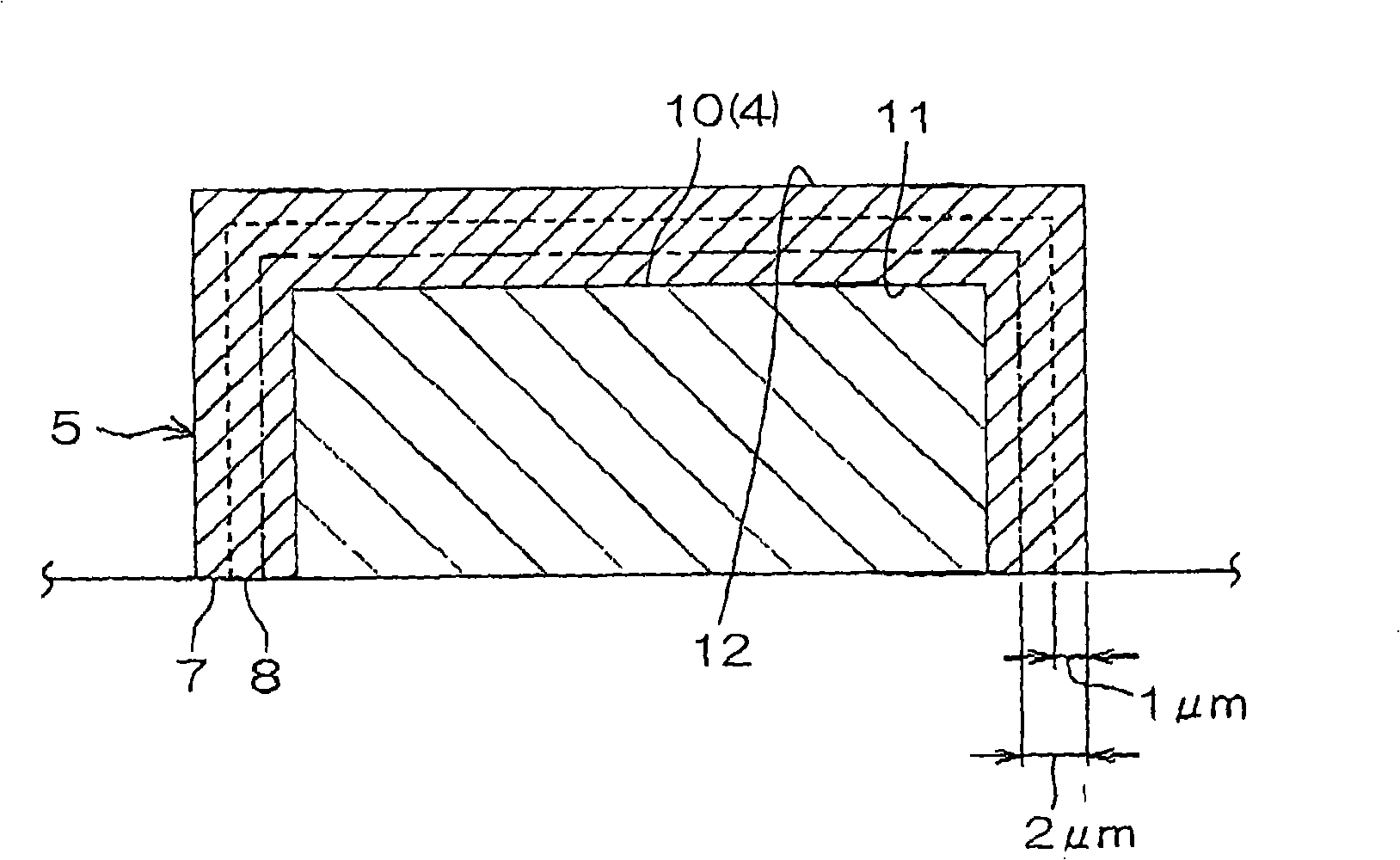
[0066] Next, a seed film was formed by sequentially forming a chromium thin film with a thickness of 50 nm and a copper thin film with a thickness of 100 nm by sputtering. Then, after forming the plating protective layer of the pattern opposite to the conductor pattern on the upper surface of this kind of film, a conductor pattern formed of copper with a thickness of 10 μm is formed by electrolytic copper plating (refer to image 3 (c)). In addition, the width ...


PUM

PropertyMeasurementUnit
thicknessaaaaaaaaaa
thicknessaaaaaaaaaa
thicknessaaaaaaaaaa

Abstract

A wired circuit board includes an insulating layer, a conductive pattern made of copper formed on the insulating layer and a covering layer made of an alloy of copper and tin to cover the conductive pattern. An existing ratio of tin in the covering layer increases in accordance with a distance from an inner surface adjacent to the conductive pattern toward an outer surface being not adjacent to the conductive pattern. An atomic ratio of copper to tin in the outer surface of the covering layer is more than 3.

Description

technical field [0001] The present invention relates to a wired circuit board and a manufacturing method thereof. Background technique [0002] Conventionally, wired circuit boards have been widely used in the fields of various electric appliances and electronic appliances. Such a wired circuit board includes an insulating base layer, a conductive pattern made of copper formed on the insulating base layer, and a cover insulating layer formed on the insulating base layer in a state of covering the conductive pattern. [0003] In such a wired circuit board, if electricity is applied for a long period of time under high temperature and high humidity, ion migration of copper in the conductive pattern to the insulating covering layer occurs, and a short circuit may occur between the conductive patterns. [0004] Therefore, in order to prevent ion migration, for example, a flexible printed circuit board (for example, referring to Japanese Patent Application Laid-Open No. 2006-27...

Claims


Application Information

Patent Timeline
Patent Type & Authority Applications(China)
IPC IPC(8): H05K1/02H05K3/22
CPCH05K2203/1105H05K3/28H05K3/244Y10T29/49117
Inventor 大薮恭也V·塔维普斯皮波恩安部勇人中村和哉龟井胜利内藤俊树
Owner NITTO DENKO CORP
Why Eureka
Try Eureka