Characteristic spectrum identification chip, manufacturing method thereof and detection device using the chip

A characteristic spectrum and chip technology, which is applied in the field of semiconductor chips, can solve the problems of expensive and complex processing and analysis devices of the adjustment mechanism, and achieve the effects of low cost, small size and easy operation

Inactive Publication Date: 2009-03-04
邵剑心 +1
View PDF0 Cites 19 Cited by
  • Summary
  • Abstract
  • Description
  • Claims
  • Application Information

AI Technical Summary

Problems solved by technology

Modern general-purpose measuring equipment can even give the emission or absorption characteristics of the sample in a wide continuous spectral range, but it also requires sophisticated and complex adjustment mechanisms, broadband spectroscopic devices and sensors, and expensive and complex processing and analysis devices. Wait
Therefore, the cost and operational complexity of these instruments make them suitable for use in only a small number of specialized medical settings

Method used


Image

  • Characteristic spectrum identification chip, manufacturing method thereof and detection device using the chip
  • Characteristic spectrum identification chip, manufacturing method thereof and detection device using the chip
  • Characteristic spectrum identification chip, manufacturing method thereof and detection device using the chip

Examples


Embodiment Construction

[0030] Exemplary embodiments of the present invention will be described below in conjunction with the accompanying drawings, so as to better understand the purpose, technical solutions and advantages of the present invention. In the description of the present application, the same reference numerals denote the same elements.

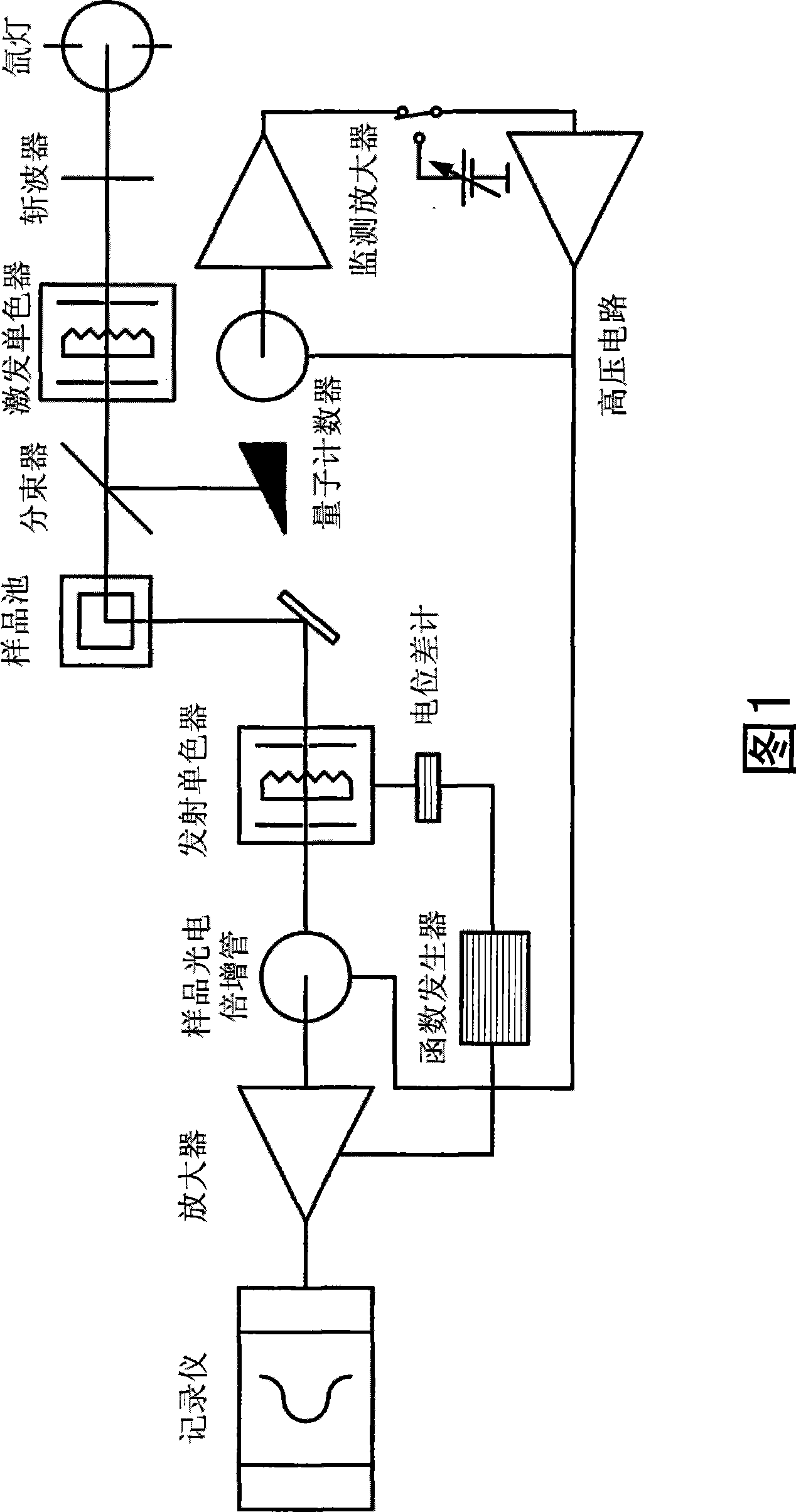
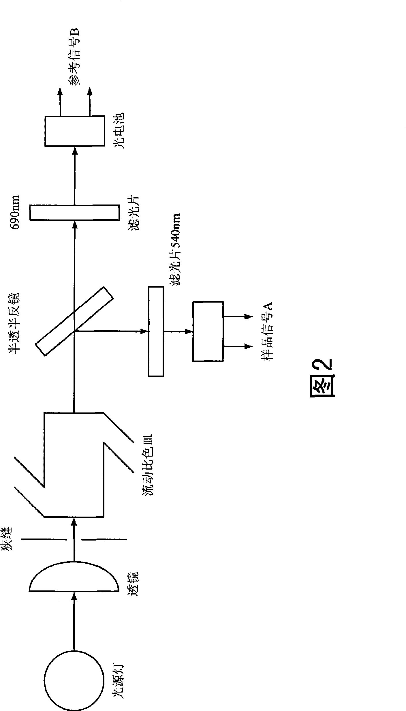
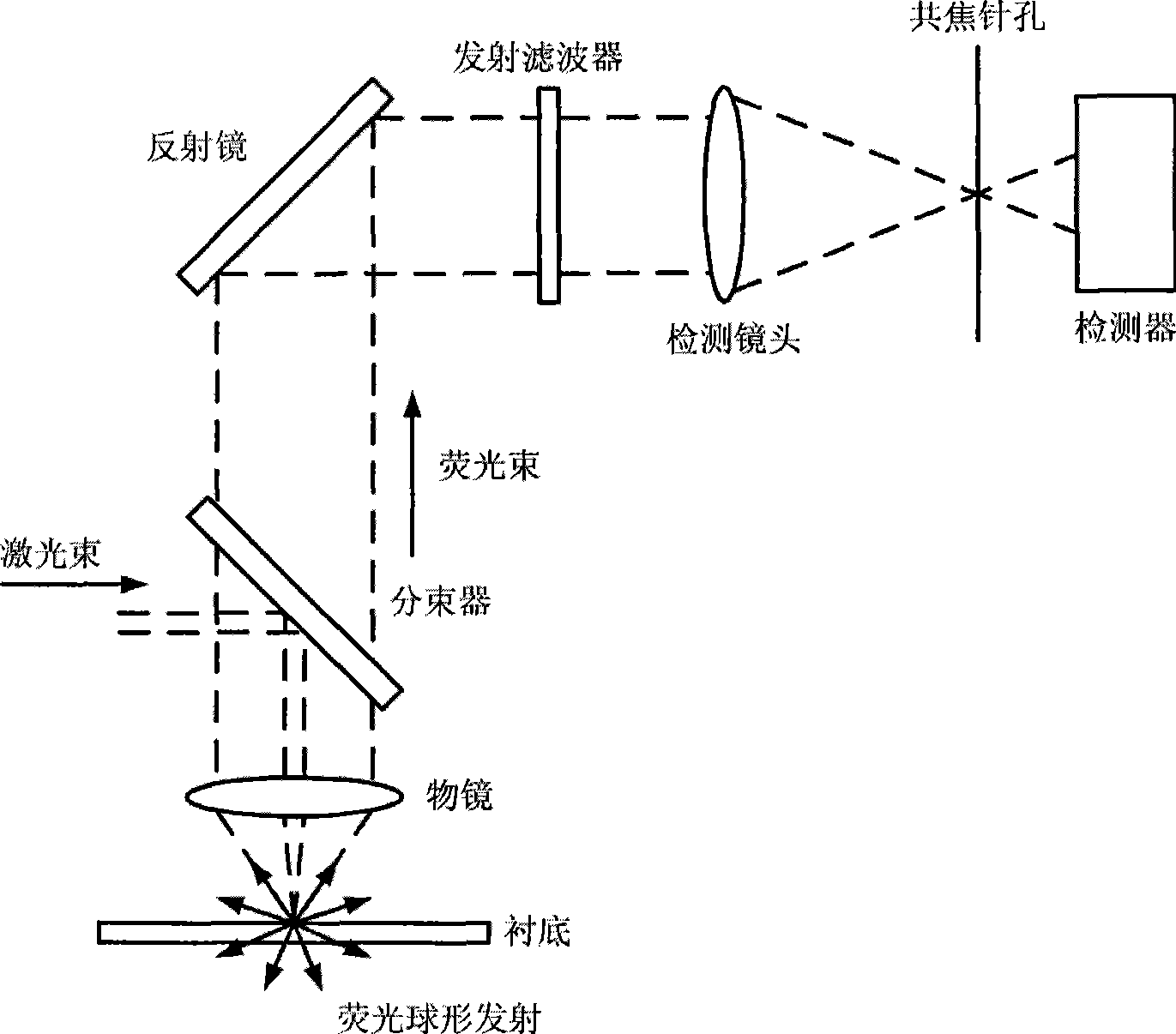
[0031] In the spectral detection process of biological samples, there are usually only one or two spectral lines (that is, one or two wavelengths) that really play a decisive role in the detection results in the entire measurement spectral range. This spectral line is called the characteristic spectrum (characteristic wavelength) . As long as the detector can selectively allow the detector to only receive the light energy of this characteristic spectrum, the desired detection effect can be obtained. Therefore, for household applications, for example, as long as the detection of several characteristic wavelengths can be achieved at a relatively low cost,...


PUM

PropertyMeasurementUnit
thicknessaaaaaaaaaa
thicknessaaaaaaaaaa
diameteraaaaaaaaaa

Abstract

The invention discloses a semiconductor chip used for characteristic spectrum discrimination and a manufacture method thereof, as well as a characteristic spectrum discrimination device and a biochip scanning device using the chip to measure absorption spectroscopy and fluorescence spectrum. According to the invention, the chip used for characteristic spectrum discrimination comprises an array semiconductor optical sensor, the array structure of which comprises at least a detection pixel and at least a reference pixel; the chip also comprises at least one optical filter plate, and the surface of each detection pixel is covered by a corresponding optical filter plate. Each optical filter plate has characteristic wavelength, thus leading the wavelength which takes the characteristic wavelength as the center in a predetermined width range to transmit through the optical filter plate, while the wavelength beyond the width range not to transmit. According to the invention, the semiconductor technology can be used for manufacturing the chip for characteristic spectrum discrimination at low cost and an absorption spectroscopy apparatus, a fluorescence spectrum apparatus and a biological microarray chip, with small volume, can be conveniently manufactured at low cost.

Description

technical field [0001] The invention relates to a semiconductor chip, in particular to a semiconductor chip for characteristic spectrum identification. The invention also relates to a manufacturing method of the chip and a detection device using the chip, especially a characteristic spectrum identification device for absorption spectrum and fluorescence spectrum and a biological chip scanning device. Background technique [0002] At present, optical detection technology has become one of the important means in biological detection, especially spectral detection technology. For example, detection of samples (such as blood samples, urine samples, etc.) by means of molecular absorption spectroscopy, atomic absorption spectroscopy, fluorescence spectroscopy, and Raman spectroscopy can provide some very useful biological information. In recent years, the rapid development of DNA gene sequencing and gene diagnosis has also been applied to fluorescence spectrum detection technolog...

Claims


Application Information

Patent Timeline
Patent Type & Authority Applications(China)
IPC IPC(8): H01L27/146H01L21/82G01N21/31G01N21/64G01J3/02
Inventor 邵剑心樊斌
Owner 邵剑心
Why Eureka
Try Eureka