Digital type silicon optical waveguide switch based on narrow slit waveguide

A slit waveguide and waveguide switch technology, applied in the field of digital silicon optical waveguide switches, can solve the problems of limited application range, low extinction ratio, large absorption loss, etc., so as to improve modulation efficiency, shorten device structure, and increase branch spacing. Effect

Inactive Publication Date: 2009-04-15
ZHEJIANG UNIV
View PDF0 Cites 12 Cited by
  • Summary
  • Abstract
  • Description
  • Claims
  • Application Information

AI Technical Summary

Problems solved by technology

However, the problem of slow thermo-optic modulation has not been solved, which seriously limits its application range.
Since the silicon material has no direct electro-optic effect

Method used


Image

  • Digital type silicon optical waveguide switch based on narrow slit waveguide
  • Digital type silicon optical waveguide switch based on narrow slit waveguide
  • Digital type silicon optical waveguide switch based on narrow slit waveguide

Examples


Embodiment 1

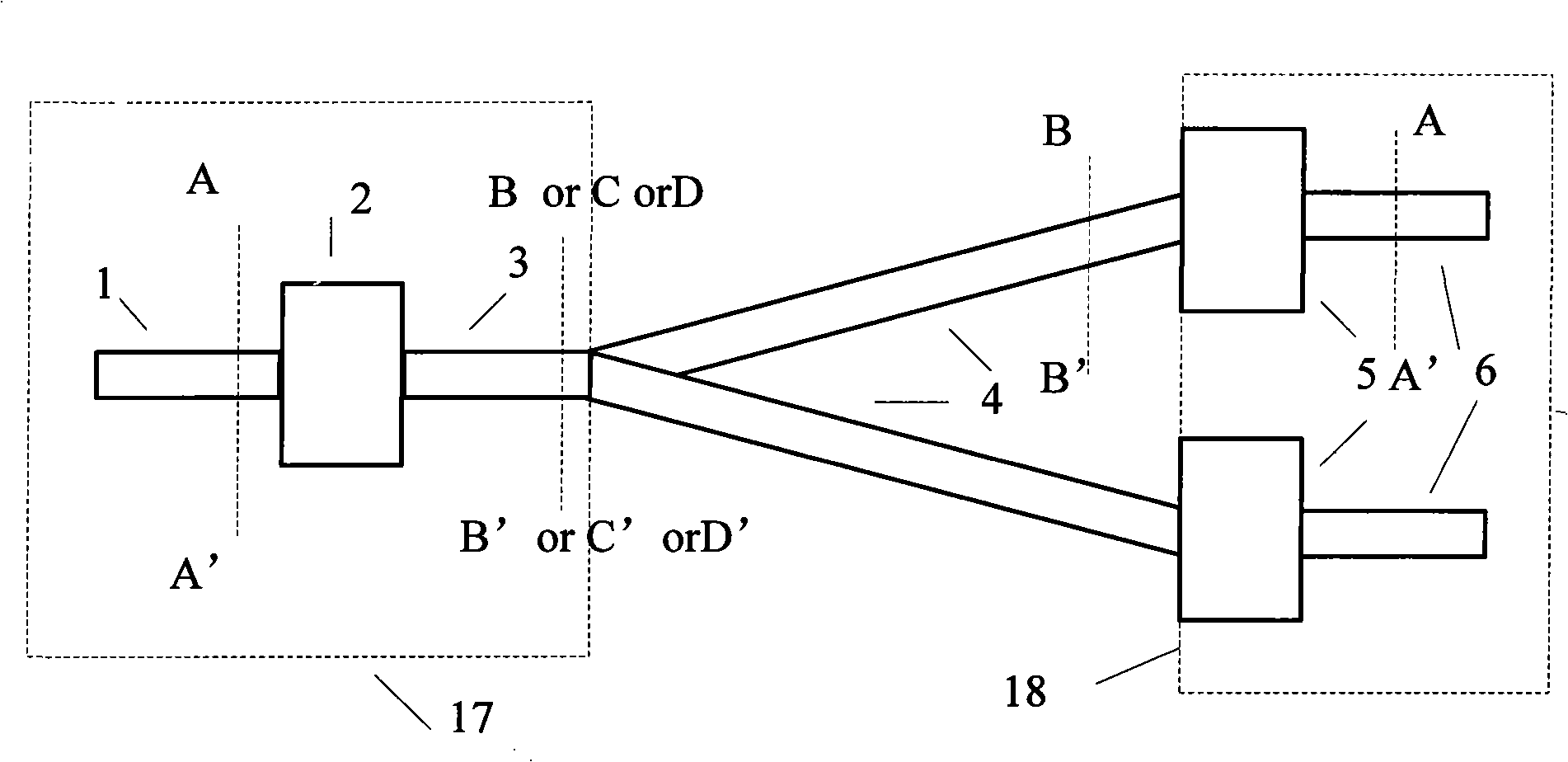
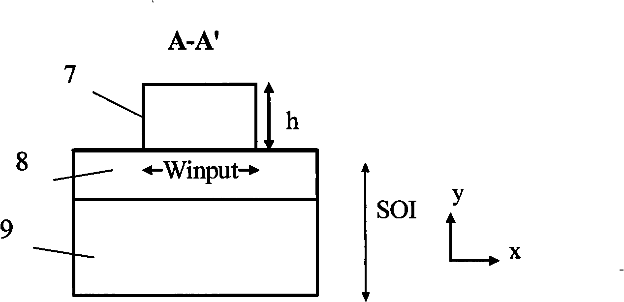
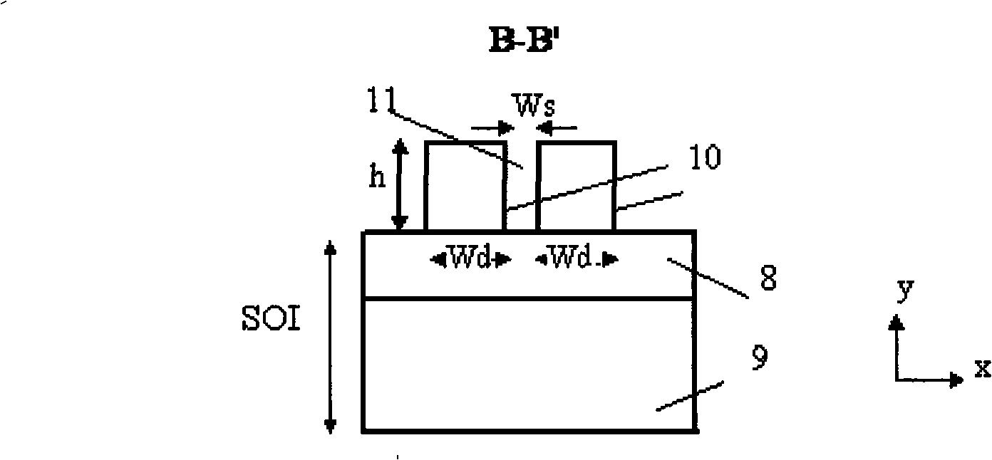
[0046] see Figure 10 As shown, a digital silicon optical waveguide switch with branch arms formed by symmetrical bifurcation of a single slit. Take an SOI sheet with a silicon thickness of 340 nm on the top layer and a silicon dioxide buffer layer 8 with a thickness of 1 micron, thermally oxidize a layer of silicon dioxide on the top layer as a mask, and use the E-beam direct writing method to etch the device structure . Including the input single-mode waveguide 1, introducing a single silicon waveguide to form a complementary tapered tapered waveguide pair 12 to form the first group of mode spot conversion structure 2, a section of waveguide 3 before the branch using a single slit, and two slit waveguide structures The branch arm 4 also introduces a single silicon waveguide to form a second group of mode speckle conversion structures 5 composed of complementary tapered tapered waveguide pairs 12 and two output single-mode waveguides 6 . The inner silicon waveguides 16 of t...

Embodiment 2

[0049] see Figure 11 As shown, the digital silicon optical waveguide switch is formed by double slit symmetrical bifurcation. Take an SOI sheet with a silicon thickness of 340 nm on the top layer and a silicon dioxide buffer layer 8 with a thickness of 1 micron, thermally oxidize a layer of silicon dioxide on the top layer as a mask, and use the E-beam direct writing method to etch the device structure . Including the input single-mode waveguide 1, the first group of mode spot conversion structures 2 formed by introducing two silicon waveguides to form a complementary tapered tapered waveguide pair 14 or the second mode spot conversion structure 15 of a hollow waveguide formed by a direct bifurcation gradient, using A section of waveguide 3 before the branch of the double slit, two branch arms 4 of the slit waveguide structure, introduce a single silicon waveguide to form a complementary tapered tapered waveguide pair 12 to form the second group of mode spot conversion struc...

Embodiment 3

[0052] see Figure 12 As shown, the digital silicon optical waveguide switch with branch arms formed by symmetrical bifurcation of multiple slits is illustrated by taking three slits as an example. Take an SOI sheet with a silicon thickness of 340 nm on the top layer and a silicon dioxide buffer layer 8 with a thickness of 1 micron, thermally oxidize a layer of silicon dioxide on the top layer as a mask, and use the E-beam direct writing method to etch the device structure . Including the input single-mode waveguide 1, the first group of mode spot conversion structures 2 composed of the first mode spot conversion structure 13 of the hollow waveguide formed by direct bifurcation and gradual change, a section of waveguide 3 before the branch using three slits, and two slits The branch arm 4 of the slot waveguide structure introduces a single silicon waveguide to form a second group of mode-spot conversion structures 5 composed of complementary tapered tapered waveguide pairs 12...


PUM

PropertyMeasurementUnit
Thicknessaaaaaaaaaa
Thicknessaaaaaaaaaa

Abstract

The invention discloses a slit waveguide-based digital type silicon optical waveguide switch. The switch comprises an input waveguide structure, two branch arms of a slit waveguide structure and an output waveguide structure; the three structures are sequentially connected, a waveguide at two sides of the slit of the two branch arms of the slit waveguide structure is a silicon waveguide, the slit is filled with an electro-optic material, and the width of the two branch arms is symmetrical or asymmetrical. An input single-mode waveguide is connected with the waveguide in front of the branch by a first set of mode-spot conversion structures, and the branch arms are connected with an output single-mode waveguide by a second set of mode-spot conversion structures. The slit is filled with a low-refractive index electro-optic material by the introduced slit waveguide, thus enlarging modulation means and introducing direct electro-optic modulation; in addition, as the silicon waveguide in naturally electrical isolation at two sides of the slit is taken as an electrode, the spacing between the electrode and a modulation area is shortened. As multi-slit is introduced, the branch spacing between the two branch arms can be increased under the condition of the same device length. The switch structure is integrated into the CMOS processing technology.

Description

technical field [0001] The invention relates to an optical communication device, in particular to a digital silicon optical waveguide switch based on a slit waveguide. Background technique [0002] Optical switches are one of the important components in optical communication and optical information processing systems. The optical switches that have been realized so far include traditional mechanical structure optical switches, switches based on micro-opto-electromechanical systems, liquid crystal optical switches, waveguide optical switches, semiconductor optical amplifier optical switches, etc. Among them, the waveguide optical switch developed by integrated photonic technology has the advantages of low driving voltage, compact structure, large-scale array and integration, and is an important development direction of optical switches. [0003] Waveguide optical switches can be divided into directional coupler type, interference type, digital type and other types. Among th...

Claims


Application Information

Patent Timeline
IPC IPC(8): G02B6/35
Inventor 肖司淼王翔王帆郝寅雷江晓清王明华杨建义
Owner ZHEJIANG UNIV
Why Eureka
Try Eureka