

Multi-chip common power supply/grounding structure for printed circuit board
A printed circuit board and grounding structure technology, which is applied in the directions of printed circuit components, multi-layer circuit manufacturing, and electrical connection printed components, can solve problems such as long decoupling efficiency distance, complex design, and isolation performance impact, and achieve parasitic parameters The effect of small size, short connection, and extended high-frequency performance
- Summary
- Abstract
- Description
- Claims
- Application Information
AI Technical Summary
Problems solved by technology
Method used
Image

Examples
Embodiment Construction
[0023] In order to make the object, technical solution and advantages of the present invention clearer, the implementation manner of the present invention will be further described in detail below in conjunction with the accompanying drawings.
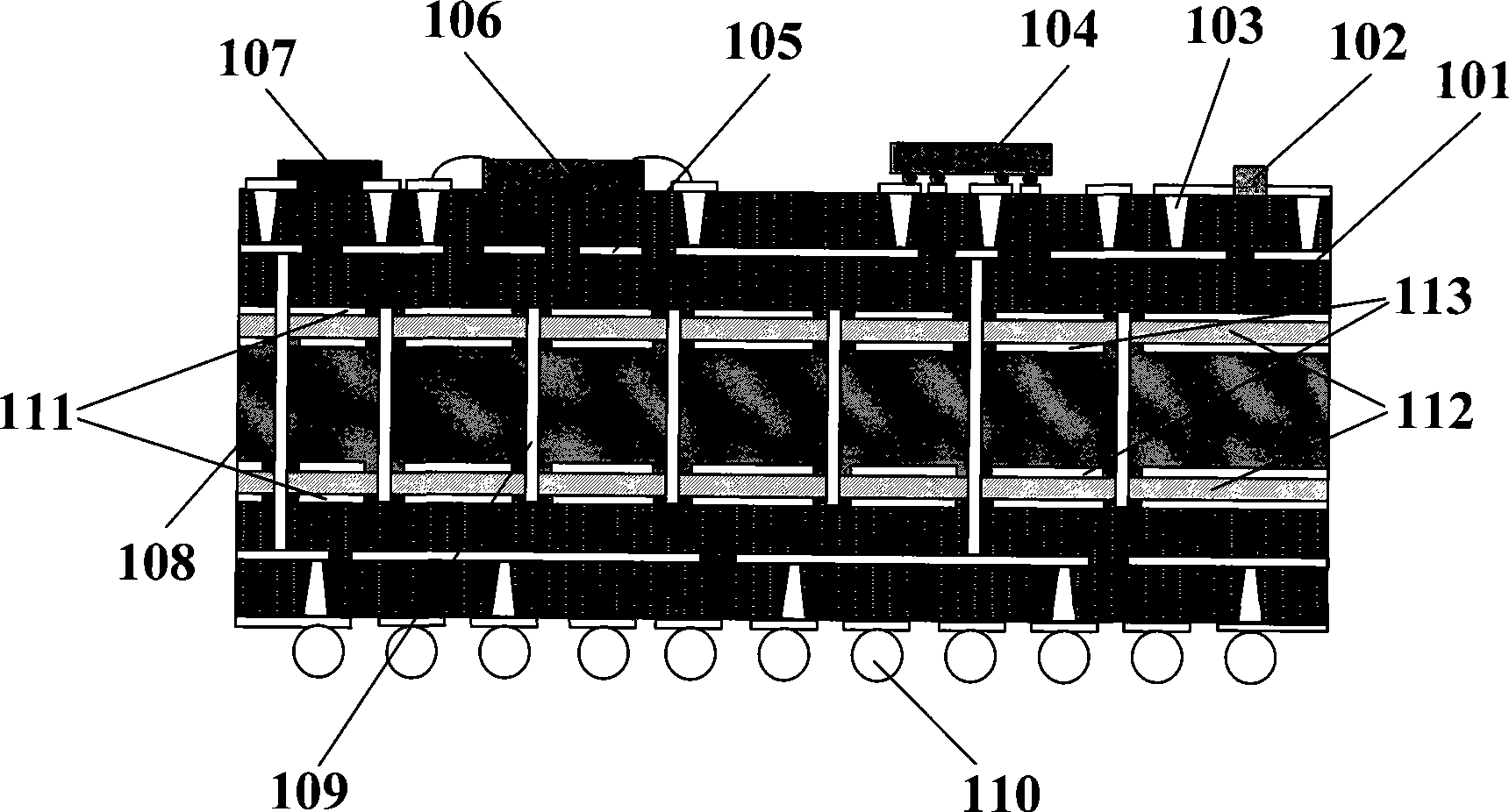
[0024] see figure 1 , the embodiment of the present invention provides a multi-chip shared power supply / ground structure in a printed circuit board, which is a typical capacitor structure in which a certain three layers are "metal-dielectric-metal" constructed in a multi-layer printed circuit board, The medium is a high dielectric constant medium. Among them: 101—multilayer printed circuit board substrate, the dielectric material is ordinary material; 102—surface mount components; 103—blind holes for interconnection; 104—bare chips in the form of flip chips; 105—signal lines; 106 —Bare chips in the form of wire bands; 107—embedded resistors; 108—the core layer of multilayer printed circuit boards, and the dielectric material is ordina...
PUM
 Abstract
Description
Claims
Application Information