Electromagnetic shielding film for display device, filter having the same, and method of fabricating the same

An electromagnetic shielding film and display device technology, which is applied in the fields of magnetic/electric field shielding, optical filters, identification devices, etc., can solve the problems of poor visibility, high cost of exposure and etching processes, and high cost of materials to achieve high visibility , the effect of excellent electromagnetic wave blocking ability

Inactive Publication Date: 2009-05-27
SAMSUNG CORNING CO LTD
View PDF0 Cites 9 Cited by
  • Summary
  • Abstract
  • Description
  • Claims
  • Application Information

AI Technical Summary

Problems solved by technology

[0012] The main problem with the etch method is that the exposure and etch process is expensive to process, and the material is also expensive since 90% or more of the copper is removed by etching
Due to these problems, a combined printing and plating type method was developed, but there is also a problem in that since the printed wiring is difficult to be as accurate as the etching method, the wiring width becomes large, which deteriorates visibility and increases defects Proportion
[0014] Further, transparent conductive films have a problem in that they are not as good at blocking electromagnetic waves as compared with metal mesh films.

Method used


Image

  • Electromagnetic shielding film for display device, filter having the same, and method of fabricating the same
  • Electromagnetic shielding film for display device, filter having the same, and method of fabricating the same
  • Electromagnetic shielding film for display device, filter having the same, and method of fabricating the same

Examples


Embodiment Construction

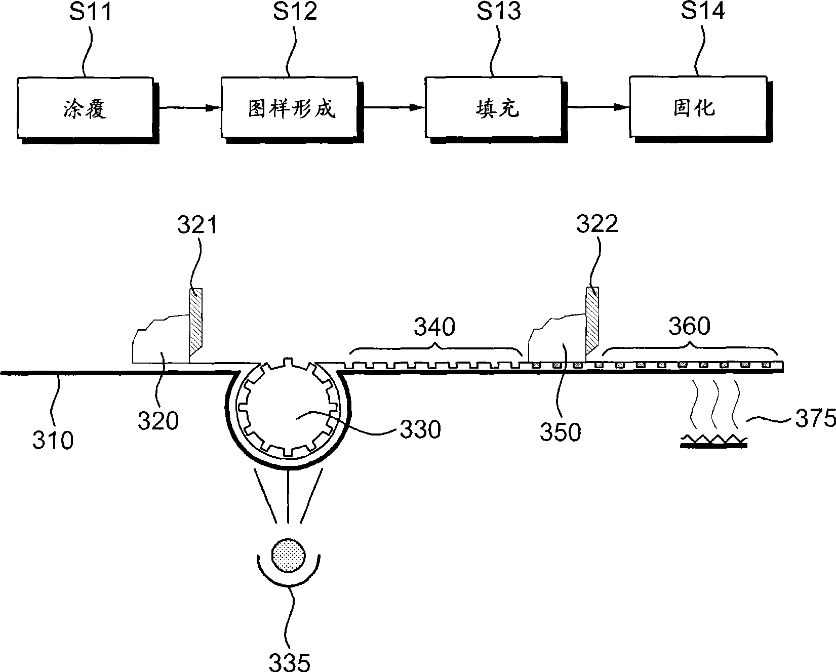
[0034] Now, the present invention will be described more fully hereinafter with reference to the accompanying drawings that show exemplary embodiments of the invention.

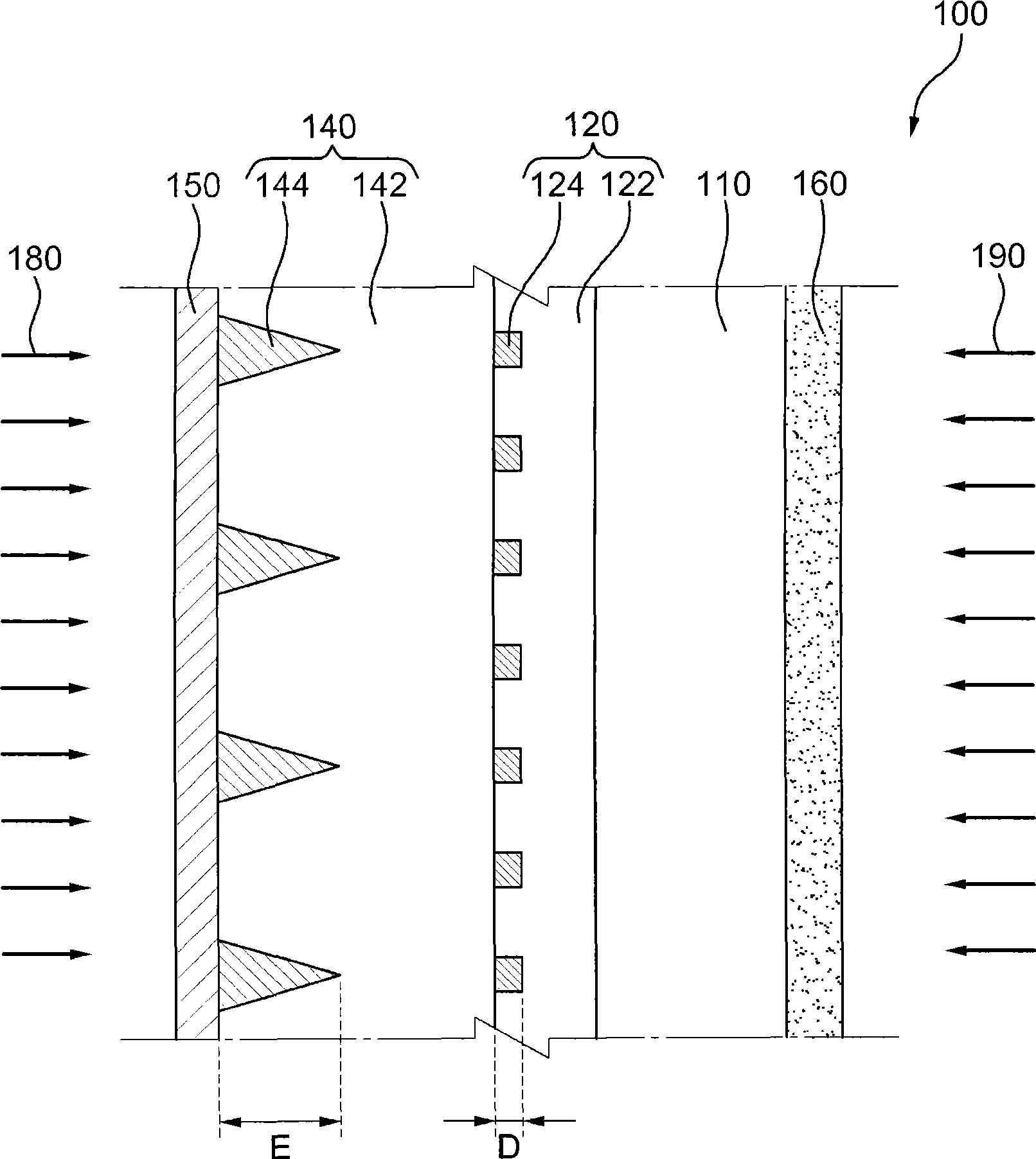
[0035] Although not shown in the drawings, a PDP according to an embodiment of the present invention includes a housing; a cover covering the housing; a drive circuit board housed in the housing; unit and has a fluorescent layer; and a PDP filter. The light emitting cells are filled with discharge gas. The discharge gas may be, for example, Ne—Xe-based gas or He—Xe-based gas. The panel assembly basically emits light in a manner similar to a fluorescent lamp in which gas discharge occurs in a light emitting unit to emit ultraviolet rays from the discharge gas, and then the ultraviolet rays excite fluorescent layers to generate visible light.

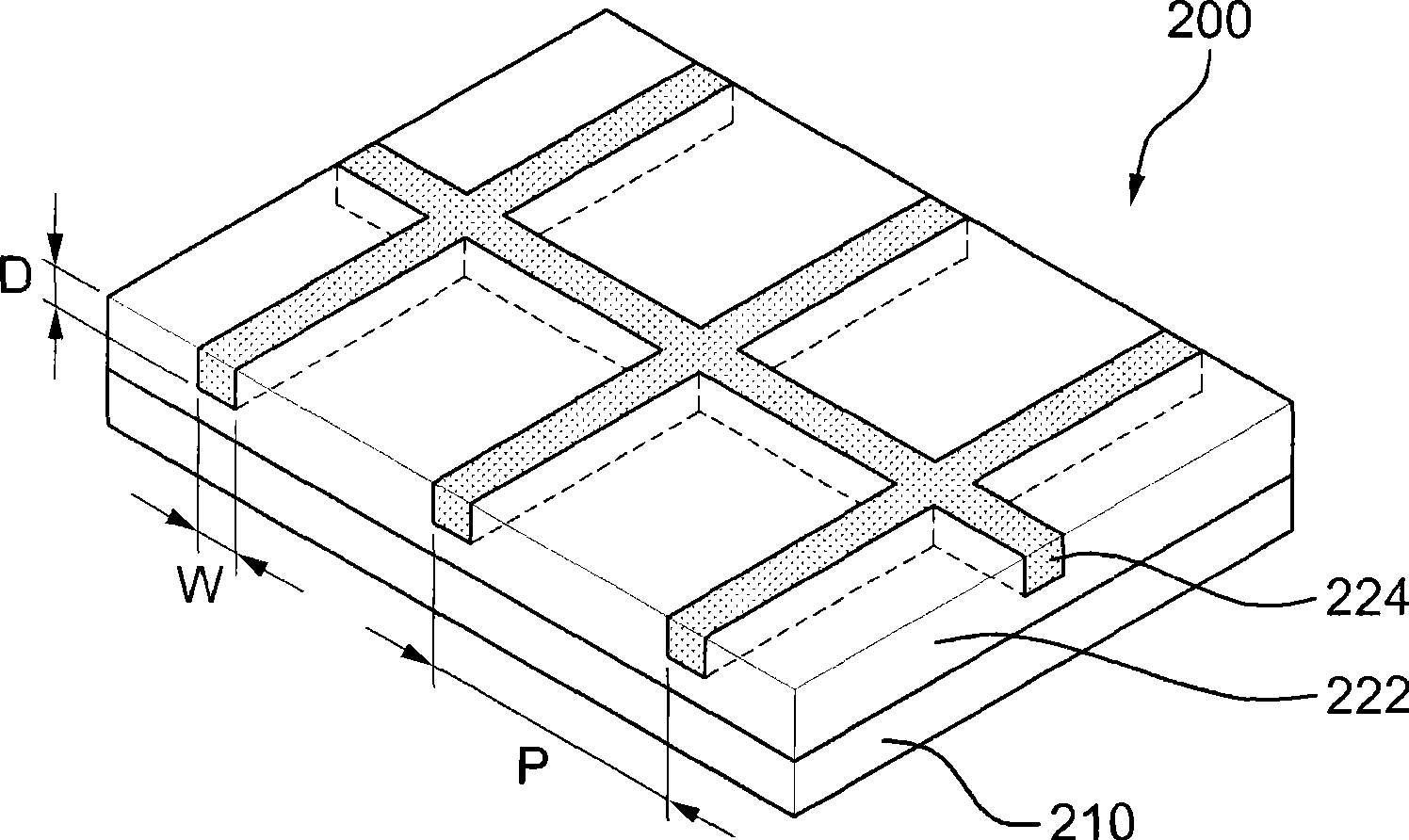
[0036] The PDP filter is disposed in front of the front substrate of the panel assembly. The PDP filter may be disposed separately from or in contact with the front s...


PUM

PropertyMeasurementUnit
depthaaaaaaaaaa
widthaaaaaaaaaa
refractive indexaaaaaaaaaa

Abstract

An electromagnetic shielding film for a display device includes a transparent, resinous first base, an intaglio pattern formed on at least one side of the first base, and an electromagnetic shielding pattern containing a conductive material with which the intaglio pattern is filled. A method of fabricating an electromagnetic shielding film for a display device, includes the steps of coating a first curable resin on one surface of a transparent backing, forming an intaglio pattern on the first curable resin using a patterning roll and curing the first curable resin, filling the intaglio pattern with a second curable resin containing a conductive material, and curing the second curable resin.

Description

[0001] Cross References to Related Applications [0002] This application claims the benefit of Korean Patent Application 2007-0118503 filed with the Korean Intellectual Property Office on November 20, 2007, the disclosure of which is hereby incorporated by reference. technical field [0003] The present invention relates to an electromagnetic shielding film for a display device, an optical filter having the film and a manufacturing method thereof, and more particularly relates to an electromagnetic shielding film for a display device which can be manufactured through a simple process and can improve electromagnetic wave blocking capability , Optical filter having the film and its manufacturing method. Background technique [0004] Display devices include televisions, personal computer monitors, portable display devices, and the like. Display devices have recently become larger in size and thinner. [0005] Accordingly, Flat Panel Display (FPD) devices, such as Plasma Disp...

Claims


Application Information

Patent Timeline
Patent Type & Authority Applications(China)
IPC IPC(8): G02B5/20H01J17/49H05K9/00B32B3/08B32B7/02C08K3/08C08K3/22C08L65/00C08L71/10G02B5/22G09F9/00
CPCH01J11/10H01J2211/446H01J11/44Y10T428/2457Y10T428/2462G02B5/20H05K9/00
Inventor 金义洙孙仁成
Owner SAMSUNG CORNING CO LTD
Why Eureka
Try Eureka