Photoetching development method

A technology of lithography and photoresist, which is applied in the direction of microlithography exposure equipment, photosensitive material processing, and photolithography process exposure device, etc. It can solve the problems affecting the etching process and photoresist residual interconnection, etc.

Inactive Publication Date: 2009-06-03
SHANGHAI HUA HONG NEC ELECTRONICS
View PDF0 Cites 6 Cited by
  • Summary
  • Abstract
  • Description
  • Claims
  • Application Information

AI Technical Summary

Problems solved by technology

There are two dimensions in the photolithographic pattern: the characteristic dimension D1 of the photoresist pattern and the characteristic dimension D2 of t

Method used


Image

  • Photoetching development method
  • Photoetching development method
  • Photoetching development method

Examples


Embodiment Construction

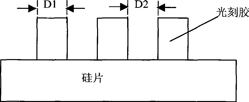
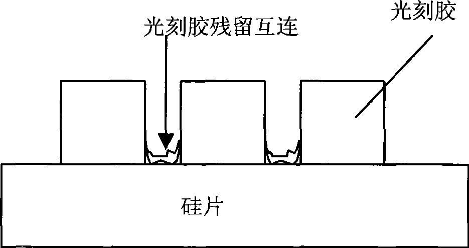
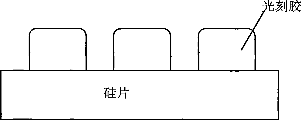
[0010] The usual photolithography development methods include coating, soft baking, exposure, post-bake, development, hard baking, and measurement of photoresist patterns on silicon wafers. In the preparation method of the present invention, the photoresist patterns are The feature size D1 is set to be smaller than the target value, generally about 1% to 30% smaller than the target value, which is equivalent to making the feature size D2 of the photoresist pattern gap larger than the target value, so the ratio of the two is D1 / D2 becomes smaller, so it can avoid the formation of photoresist residue interconnection in the gap of the photoresist pattern after development; while the hard baking needs to increase the hard baking temperature, because the increase in temperature makes the photoresist slightly in the hard baking process After softening, the characteristic size of the photoresist pattern gap after hard baking is finally within the target value range. In this step, due to...


PUM


Abstract

The invention discloses a photoetching development method, comprising the steps of exposing and hard curing; the characteristic sizes of exposed photoresist patterns are less than target value; the hard curing temperature in the hard curing process is increased, so that the characteristic sizes of the gaps of hard-cured photoresist patterns are controlled in the target value range. The method effectively prevents the photoresist remaining in the gaps of the photoresist patterns to form photoresist residuals interconnection in the development process; the hard curing temperature in the hard curing process is increased, and the photoresist is softened, so that the characteristic sizes of the hard-cured photoresist patterns are larger, and the characteristic sizes of the gaps of photoresist patterns are controlled in the target value range. The invention can be widely used for the manufacturing of semiconductor devices.

Description

Technical field [0001] The invention relates to a method of photolithography development. Background technique [0002] The photolithography development process is an important technology in semiconductor manufacturing. In photolithography, the silicon wafer has gone through a series of process steps in the coating / developing machine. The upper surface of the pretreatment silicon wafer is coated with glue, glued, and baked (often called soft baking). The automatic transfer device inside the equipment transfers the silicon wafers between the operating positions. Another set of conveying device sends the glued silicon wafers one piece at a time into the alignment and exposure system. The photolithography machine directly engraves the pattern of the specific mask on the glued silicon wafer. After the exposed silicon wafer is transferred from the exposure system to the silicon wafer track system, a short post-exposure bake (commonly called post-bake) is required to provide photoresis...

Claims


Application Information

Patent Timeline
IPC IPC(8): G03F7/20G03F7/40G03F7/26H01L21/027
Inventor 陈华伦罗啸陈雄斌熊涛陈瑜
Owner SHANGHAI HUA HONG NEC ELECTRONICS
Why Eureka
Try Eureka