Zero layer alignment maker and preparation method

A technology for zero-layer alignment marks and manufacturing methods, which is applied to the photoplate-making process of the pattern surface, the photoplate-making process exposure device, optics, etc., which can solve the cumbersome process steps, affect the process progress, and increase the exposure, development and etching steps and other issues to achieve the effect of simplifying the process steps

Inactive Publication Date: 2009-06-03
SEMICON MFG INT (SHANGHAI) CORP
View PDF1 Cites 19 Cited by
  • Summary
  • Abstract
  • Description
  • Claims
  • Application Information

AI Technical Summary

Problems solved by technology

Increased exposure, development and etching steps, resultin

Method used


Image

  • Zero layer alignment maker and preparation method
  • Zero layer alignment maker and preparation method
  • Zero layer alignment maker and preparation method

Examples


Embodiment Construction

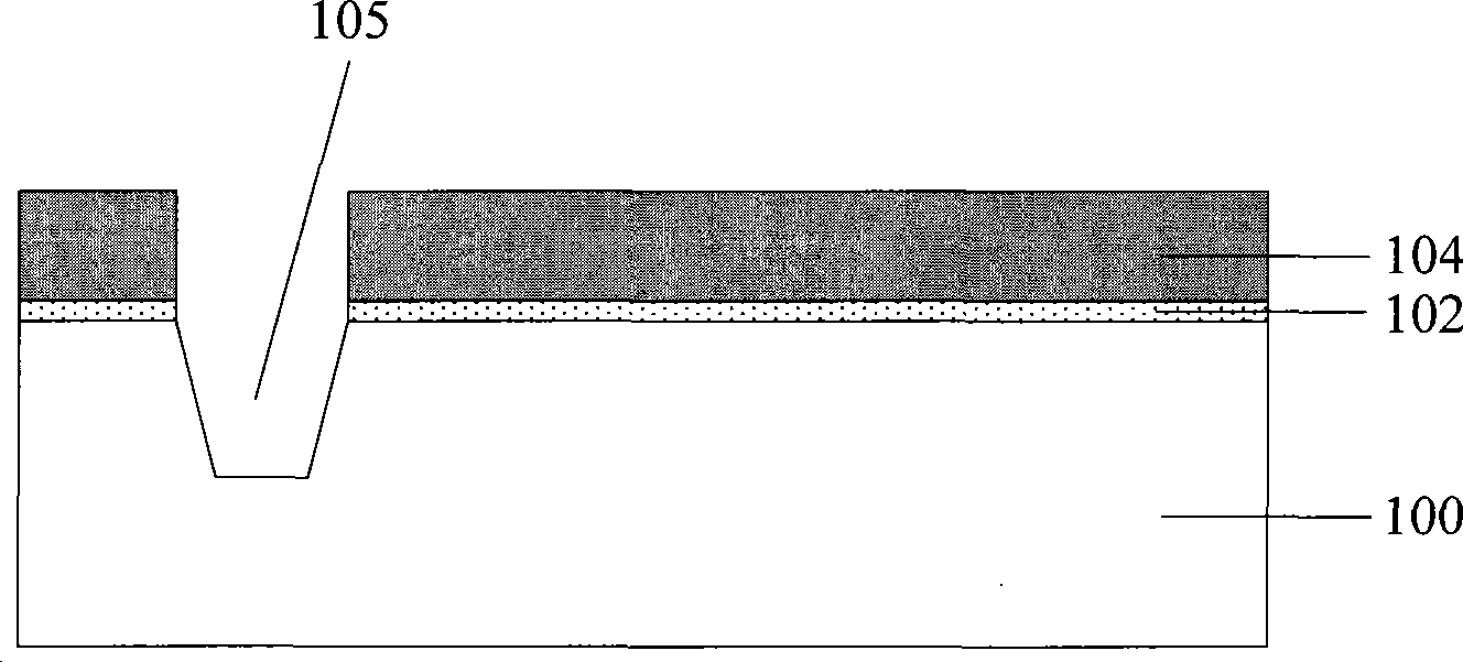
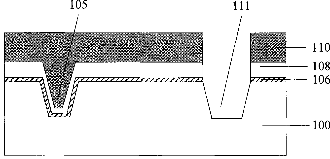
[0027] In the process of removing the corrosion barrier layer in the present invention, since there is no corrosion barrier layer on the side wall of the zero-layer alignment mark groove, the insulating dielectric layer in the zero-layer alignment mark groove can remain intact as a zero-layer alignment mark, so no The steps of exposure, development and etching need to be added to remove the insulating dielectric layer in the trench and the corrosion barrier layer under the insulating dielectric layer, so that the zero-layer alignment mark trench covering the pad oxide layer is used as the zero-layer alignment mark. The process steps are simplified.

[0028] Further, the zero-layer alignment mark and the shallow trench isolation structure are formed simultaneously, which simplifies the process steps and improves the yield.

[0029] The specific embodiments of the present invention will be described in detail below in conjunction with the accompanying drawings.

[0030] Figur...


PUM


Abstract

The invention provides a method for preparing zero layer alignment marker, comprising the steps as follows: a semiconductor underlayer which is sequentially provided with an oxidation cushion layer, a corrosion blocking layer and a photoresist is provided; a zero layer alignment marking pattern and a shallow channel pattern are defined on the photoresist layer; the photoresist layer is taken as a mask to etch the corrosion blocking layer, the oxidation cushion layer and the semiconductor underlayer and form the zero layer alignment marking channel and the shallow channel; after the photoresist layer is removed, the oxidation lining layer is formed on the internal wall of the zero layer alignment marking channel and the shallow channel; the zero layer alignment marking channel and the shallow channel are filled with insulated medium layer, thus forming the zero layer alignment marker and the shallow channel separation structure; subsequently, the corrosion blocking layer is removed. The invention also provides a zero layer alignment marker which simplifies the process steps.

Description

technical field [0001] The invention relates to the field of semiconductor devices and manufacturing, in particular to a zero-layer alignment mark and a manufacturing method. Background technique [0002] In the case of higher integration of semiconductor process and smaller process size, the complexity and difficulty of process steps are getting higher and higher. Therefore, it is necessary to use measuring equipment for process monitoring in the process to reflect problems in real time and reduce process errors. the loss caused. [0003] Photolithography is arguably one of the most critical steps in semiconductor processing. All layer patterns and doped regions related to the structure of the MOS components are determined by the photolithography process. Besides the critical dimension (CD) control, another important factor that usually determines the success or failure of the wafer photolithography process is the alignment accuracy. Such as figure 1 As shown, in order ...

Claims


Application Information

Patent Timeline
IPC IPC(8): G03F7/20G03F9/00
Inventor 肖德元刘永
Owner SEMICON MFG INT (SHANGHAI) CORP
Why Eureka
Try Eureka