Encapsulation structure and method for white light emitting diode device

A technology of light-emitting diodes and packaging structures, which is applied in the fields of electric solid-state devices, semiconductor devices, semiconductor/solid-state device manufacturing, etc., and can solve problems such as precipitation, non-recyclability, slow phosphor powder, etc.

Inactive Publication Date: 2009-06-10
GUANGDONG REAL FAITH OPTO
View PDF0 Cites 30 Cited by
  • Summary
  • Abstract
  • Description
  • Claims
  • Application Information

AI Technical Summary

Problems solved by technology

Although this method can ensure that the performance of each product will not vary too much at the time of testing, the phosphor will slowly precipitate before the LED is not cured and during the curing process.
This often leads to considerable differences in the performance of LEDs after full curing, resulting in some products whose light and color quality cannot meet the needs
Although LEDs can still work normally, these substandard products are equivalent to waste products, which can neither be recycled nor sold

Method used


Image

  • Encapsulation structure and method for white light emitting diode device
  • Encapsulation structure and method for white light emitting diode device
  • Encapsulation structure and method for white light emitting diode device

Examples


Embodiment 1

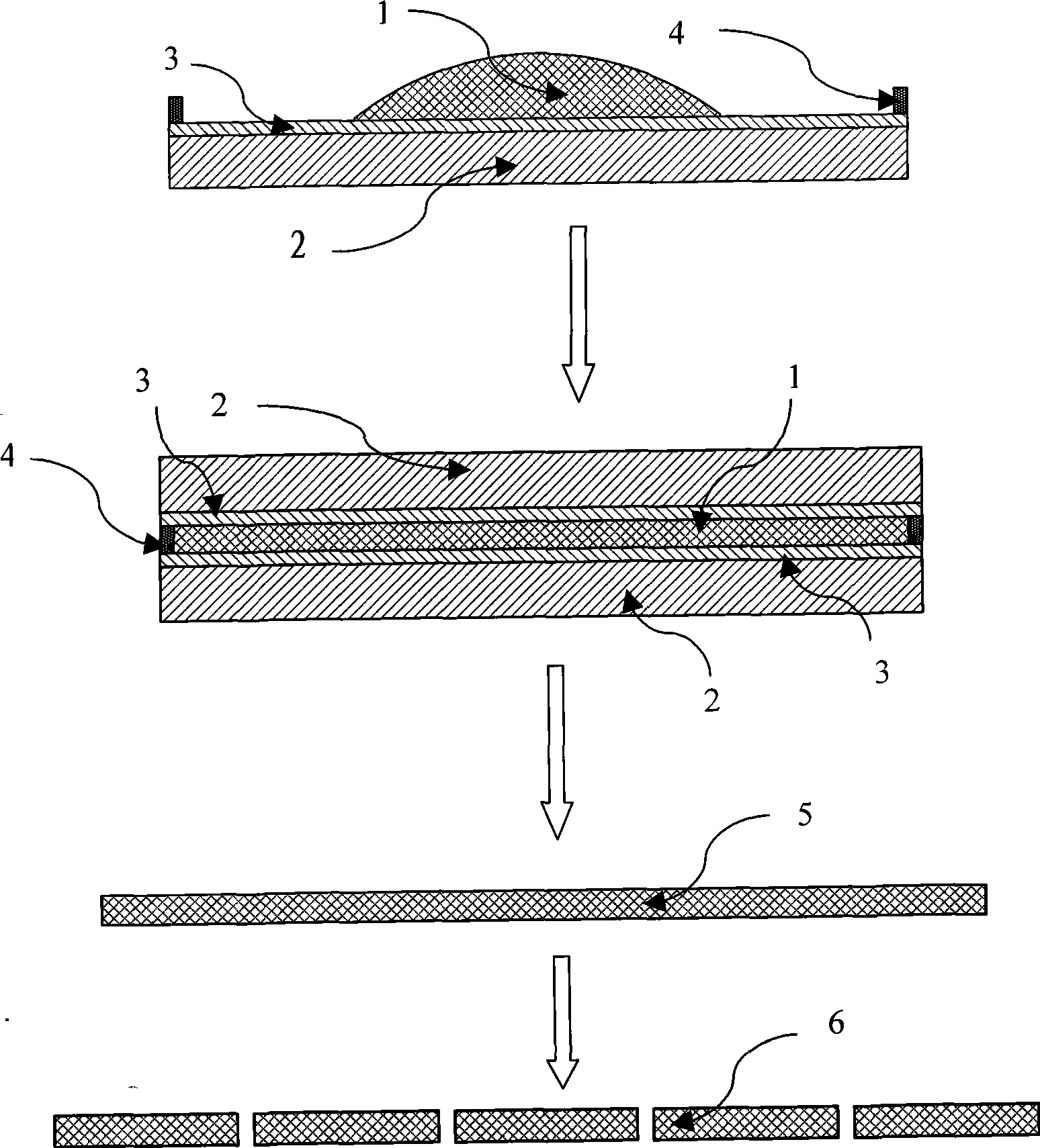
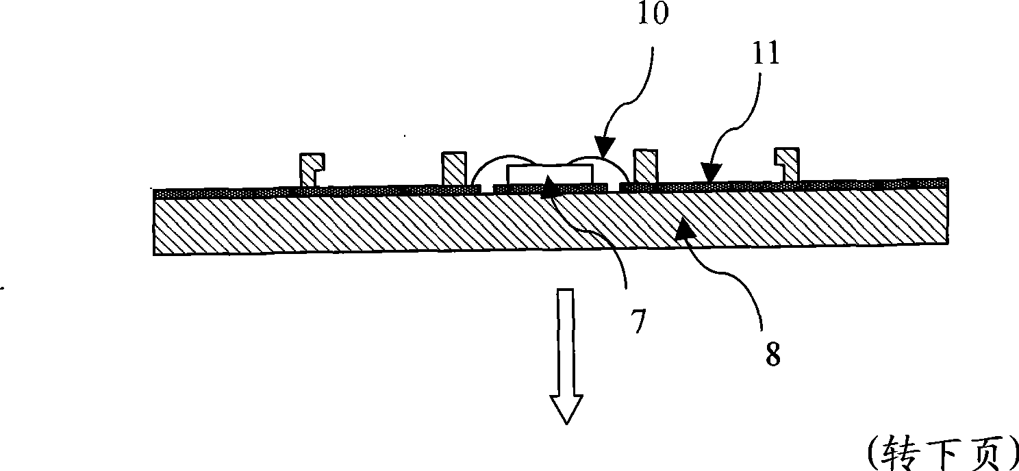
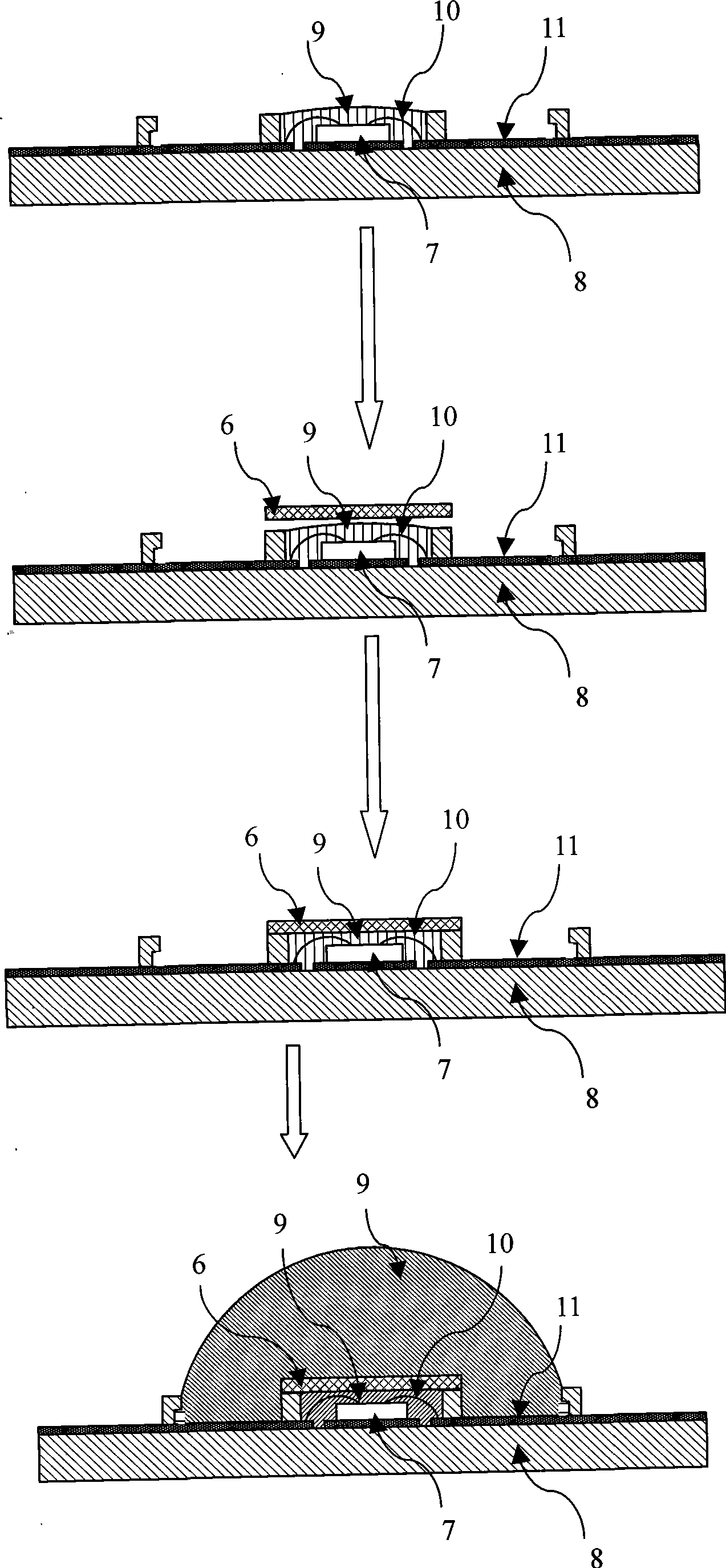
[0041] Such as figure 2 Shown is a schematic structural diagram of Embodiment 1 of the present invention. The package structure of the white light emitting diode device includes an LED chip 7 , a package shell 8 , a package silica gel 9 , a gold wire 10 and a phosphor film 6 . The LED chip 7 is a front-mounted chip, and the chip electrode can be a vertical electrode or a planar electrode, and it is a planar electrode in this embodiment. The LED chip 7 is mounted on the circuit layer 11 of the package package 8, and the package package 8 is a ceramic substrate or a metal substrate. Some structures on the packaging shell 8 can restrict the flow of the packaging silica gel 9 , so that a thin layer of packaging silica gel 9 can be coated on the surface of the chip. Phosphor film 6 is pressed on the above structure and the first layer of encapsulating silica gel 9 .

[0042] This embodiment also proposes two other methods for forming the first layer of encapsulating silica gel....

Embodiment 2

[0045] Such as image 3 Shown is a schematic structural diagram of Embodiment 2 of the present invention. The difference from Embodiment 1 is that the packaging tube 8 has a reflective cup structure, and the height of the phosphor film 6 is limited by the structure on the reflective cup, and the height can be adjusted according to the light color index.

Embodiment 3

[0047] Such as Figure 4 Shown is a schematic structural diagram of Embodiment 3 of the present invention. The difference from Example 2 is that after the first layer of encapsulating silica gel 9 is coated, the phosphor film 6 can have multiple layers, and each layer of phosphor film 6 can have thickness, concentration, phosphor type, etc. have difference.


PUM


Abstract

The invention provides a packaging structure and a method for preparing white-light LED by utilizing phosphor thin films. The packaging structure and the method are characterized in that the phosphor thin films with various different parameters are prepared in advance and cut into the size needed for packaging an LED chip; after the LED chip is pasted in a packaging tube shell, the LED chip is first coated with a layer of packaging silica gel, and then the phosphor thin film with the needed parameters is placed on the silica gel through on-line detection according to the requirement on the photochromic quality of needed white light; and finally the packaging of a whole device is completed by use of the packaging silica gel. The packaging structure and the method can conveniently regulate the photochromic quality of the white light during production, simplify and shorten a color temperature regulation process for the white-light LED. In addition, the phosphor thin films prepared in advance can avoid the problem of phosphor precipitation in a dispensing process and a silica-gel solidifying process, so that the performance consistency of the white-light LED is easy to guarantee.

Description

technical field [0001] The invention relates to a white light emitting diode, in particular to a packaging structure and method of a white light emitting diode device. Background technique [0002] Light-emitting diode (LED) is an electroluminescent device processed by semiconductor manufacturing technology. Its light-emitting mechanism is to use the recombination of electrons and holes to generate photons. This recombination effect can theoretically approach 100% quantum efficiency under continuous current and stable voltage drive. This method of electric injection can also avoid large Stokes shift, so LED has the advantages of high luminous efficiency, good color rendering, low power consumption, energy saving and environmental protection, high safety and reliability, and long service life. [0003] Since the first blue LED chip was successfully developed in 1994, there are currently two main technologies for obtaining white LEDs. One is to use high-brightness InGaN blue ...

Claims


Application Information

Patent Timeline
Patent Type & Authority Applications(China)
IPC IPC(8): H01L33/00H01L25/00H01L25/075H01L21/50H01L33/48H01L33/50
Inventor 刘胜刘宗源罗小兵王恺陈明祥甘志银金春晓
Owner GUANGDONG REAL FAITH OPTO
Why Eureka
Try Eureka