
Slew-rate control apparatus and methods for a power transistor to reduce voltage transients during inductive flyback

一种转换速率、晶体管的技术,应用在输出功率的转换装置、晶体管、功率振荡器等方向,能够解决系统执行低、干扰等问题

Inactive Publication Date: 2012-09-26
FREESCALE SEMICON INC
View PDF0 Cites 0 Cited by
  • Summary
  • Abstract
  • Description
  • Claims
  • Application Information

AI Technical Summary

Problems solved by technology

Conducted and / or radiated emissions often cause interference in other electronic devices coupled to or closest to the power switch, which can cause the overall system to perform less than expected

Method used


Image

  • Slew-rate control apparatus and methods for a power transistor to reduce voltage transients during inductive flyback
  • Slew-rate control apparatus and methods for a power transistor to reduce voltage transients during inductive flyback
  • Slew-rate control apparatus and methods for a power transistor to reduce voltage transients during inductive flyback

Examples


Embodiment Construction

[0020] The following detailed description is merely illustrative in nature and is not intended to limit the scope or application of the possible embodiments. Furthermore, there is no intention to be bound by any expressed or implied theory presented in the preceding technical field, background, brief summary or the following detailed description.

[0021] Various embodiments are described herein with the aid of functional and / or logical block components and various processing steps. It should be appreciated that such block components may be realized via any number of hardware, software, and / or firmware components configured to perform the specified functions. For reasons of brevity, conventional techniques and systems pertaining to semiconductor processing, packaging, and semiconductor devices are not discussed in detail herein.

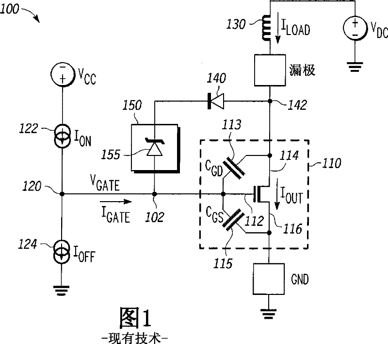
[0022] As described above, conventional power switches fail in many respects. For example, referring to FIG. 1A , a power switch 100 includes a tr...


PUM


Abstract

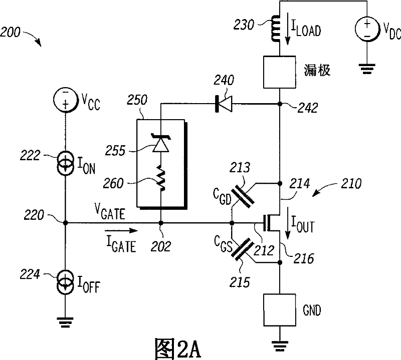
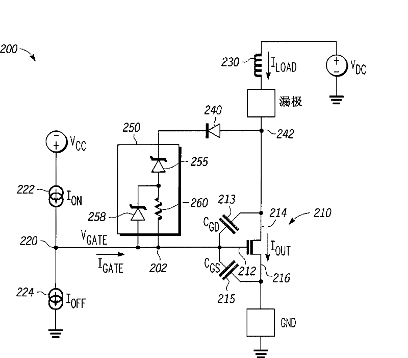
Apparatus and methods that reduce the amount of conducted / radiated emissions from a power switch (200) when a transistor (210) is switched OFF are disclosed. In addition, apparatus and methods that reduce the slew rate in a power switch when the power switch is switched off are disclosed. The apparatus comprises a transistor (210) including an inductive load (230) coupled to the transistor, a plurality of current sources (222, 224) coupled to the gate of the transistor, and a clamp (250) coupled to either the gate and the drain of the transistor, or to the gate and to ground depending on the location of the inductive load, wherein the clamp comprises a resistive element (260) to increase the voltage of the clamp when current flows through the clamp, and wherein the increased voltage causes the apparatus to include a different slew rate.

Description

technical field [0001] The present invention relates generally to semiconductor devices, and more particularly to power switches. Background technique [0002] In a power switch, when a transistor driving an inductive load is turned off, the drain voltage of the transistor increases suddenly. Sudden changes in drain voltage usually cause conducted or radiated emissions on the output lines to the inductive load. Conducted and / or radiated emissions often cause interference in other electronic devices coupled to or in immediate proximity to the power switch, which can cause the overall system to perform less than expected. [0003] Accordingly, there is a need to provide apparatus and methods that reduce the amount of conducted or radiated emissions from a power switch when the transistor is turned off. Additionally, it would be desirable to provide an apparatus and method for altering the transition time of the voltage in the power switch when the transistor is switched off....

Claims


Application Information

Patent Timeline
Patent Type & Authority Patents(China)
IPC IPC(8): H03K5/12H03K3/00H03B1/00
CPCH03K17/166H03K17/163H03K17/0822H02M2001/0029H01L2924/14H02M1/0029H01L2924/00
Inventor 保罗·T·班尼特兰德尔·C·格雷马修·D·汤普森
Owner FREESCALE SEMICON INC
Learn More