

Electric charge induction image forming method based on semiconductor layer
A technology of charge induction and imaging method, which is applied in the direction of TV, camera tube, electrical components, etc., can solve the problems of inconvenient anode replacement, difficult vacuum packaging, and poor imaging quality, so as to simplify electronic design, facilitate research, and reduce imaging link effect
- Summary
- Abstract
- Description
- Claims
- Application Information
AI Technical Summary
Problems solved by technology
Method used
Image

Examples
Embodiment Construction
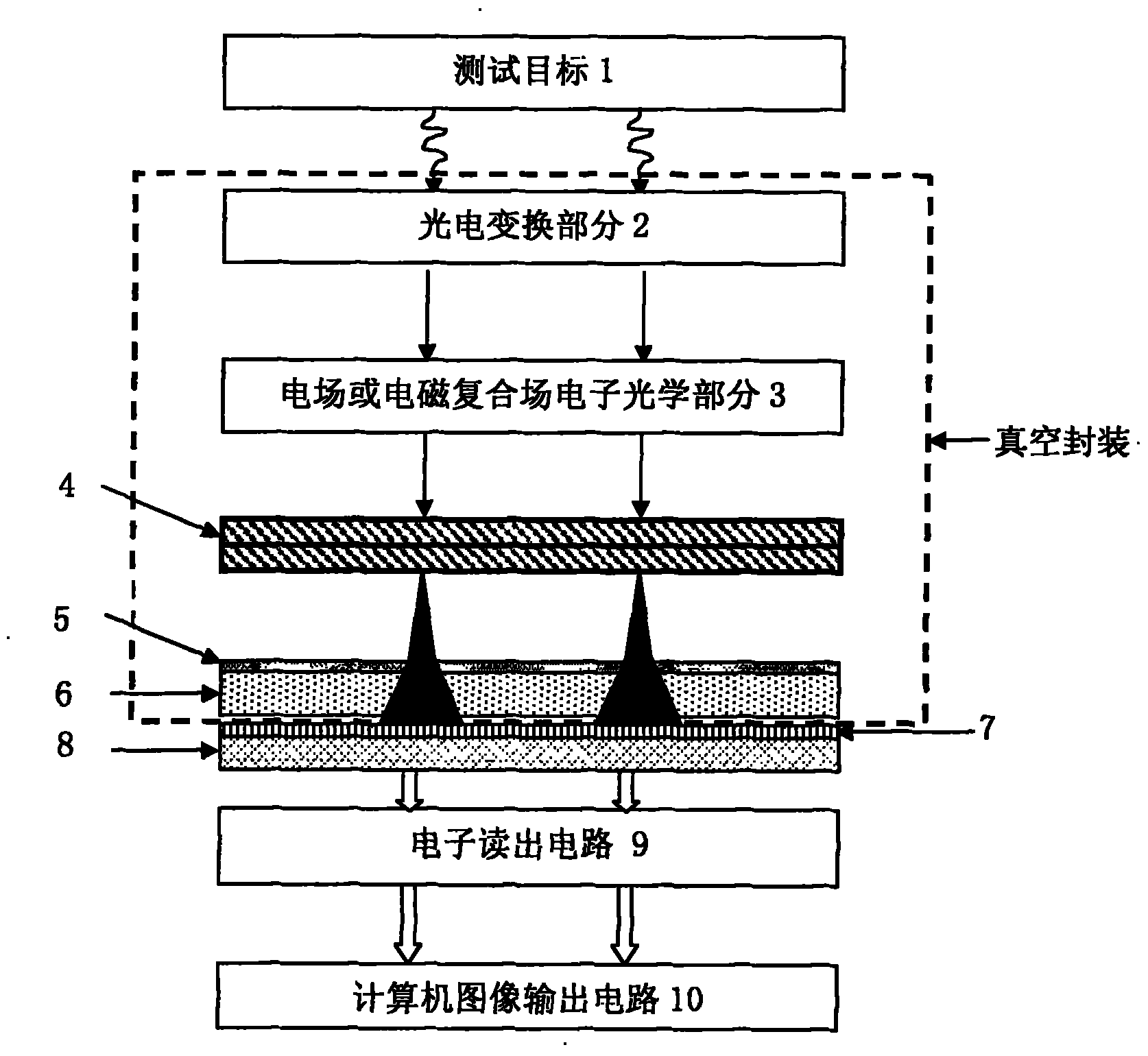
[0028] A charge-induced imaging method based on a semiconductor germanium layer can be widely applied to optoelectronic imaging devices, such as image converters, image intensifiers, single photon counting imaging detectors, etc. The structure diagram of the photoelectric imaging device using this imaging method is as follows figure 1 shown.
[0029] Concrete steps of the present invention are as follows:
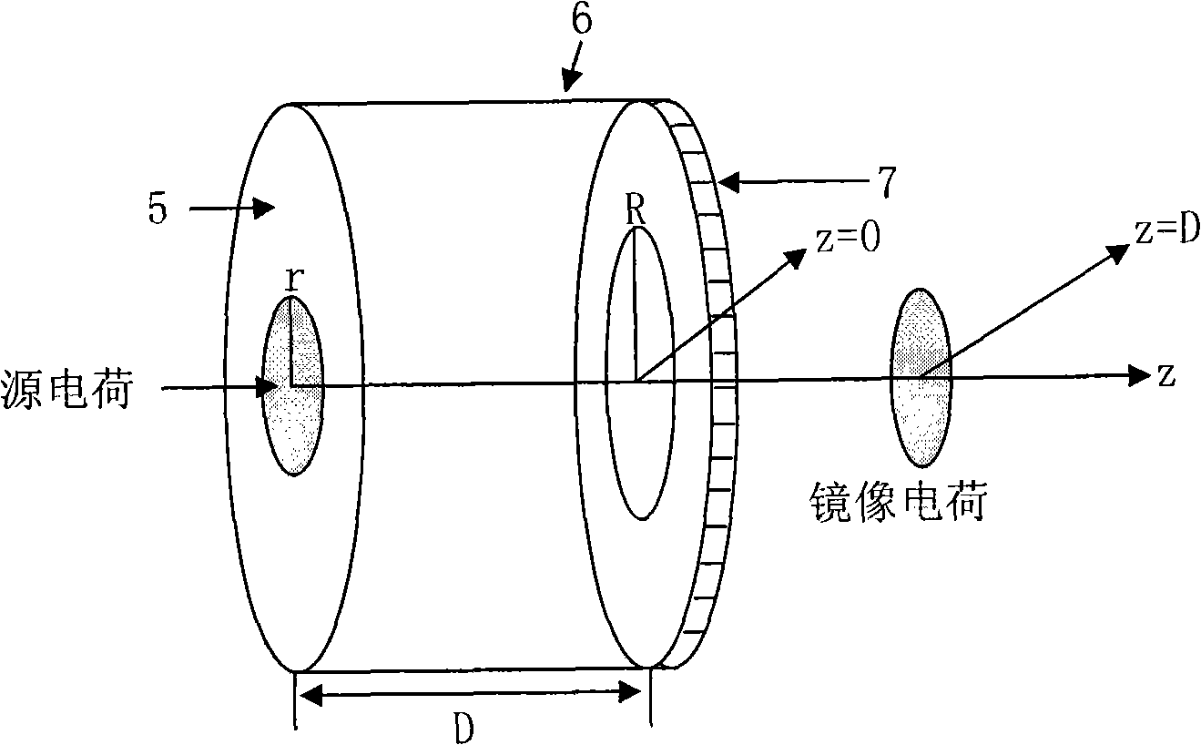
[0030] 1] Replace the phosphor screen of the photoelectric imaging device with a semiconductor germanium layer with a substrate 6, set a position-sensitive anode 7 outside the vacuum on the back of the substrate 6 of the semiconductor germanium layer, and require the square resistance range of the semiconductor germanium layer to be 100MΩ / □ ~1000MΩ / □, the thickness of the germanium layer ranges from 50nm to 400nm, and the thickness of the substrate 6 ranges from 1mm to 3mm; the substrate 6 can be made of glass-ceramics, quartz glass or alumina ceramics; Channel Array Anode...
PUM
 Abstract
Description
Claims
Application Information