Preparation method for coarsing P-GaN layer surface of LED

A surface roughening and manufacturing method technology, applied in the field of roughening technology, can solve the problems of complex process, high cost, unsatisfactory effect, etc., and achieve the effect of improved roughening effect and simple operation

Active Publication Date: 2009-07-29
EPILIGHT TECH +1
View PDF1 Cites 23 Cited by
  • Summary
  • Abstract
  • Description
  • Claims
  • Application Information

AI Technical Summary

Problems solved by technology

[0004] At present, there are two main types of treatment methods for the surface roughening of GaN-based LEDs: one is to post-treat the surface of GaN-based LEDs. etching, dry etching, imprint lithography, and selected area etching for making metal masks. For example, it is more commonly used to grow a metal layer on the surface of the P-GaN layer, and then melt the metal to form a metal layer on the surface of the P-GaN layer. bag shape, and then use this bag shape as a mask to etch to roughen the surface of the P-GaN layer. This process is more complicated and costly; In the GaN layer, cooling treatment is used to roughen the surface of the P-GaN layer. However, since the P-GaN layer is often doped with magnesium in the existing process, the surface roughening of the P-GaN layer formed by cooling is not effective. Ideal, and the difficulty of roughening is also increased after doping with magnesium

Method used


Image

  • Preparation method for coarsing P-GaN layer surface of LED
  • Preparation method for coarsing P-GaN layer surface of LED
  • Preparation method for coarsing P-GaN layer surface of LED

Examples


Embodiment Construction

[0015] The fabrication method of the present invention capable of roughening the surface of the P-GaN layer of the LED will be further described in detail through specific examples, wherein the method of the present invention is carried out by metal-organic chemical vapor deposition (MOCVD).

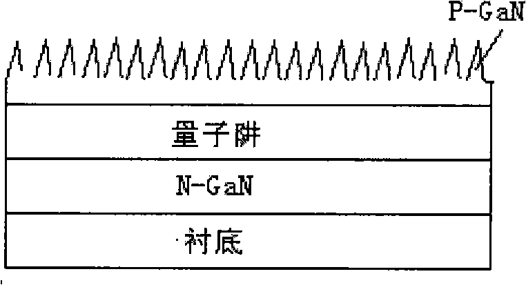
[0016] see Figure 2A to Figure 2B , the preparation method of the present invention that can roughen the surface of the P-GaN layer of LED mainly includes the following steps:

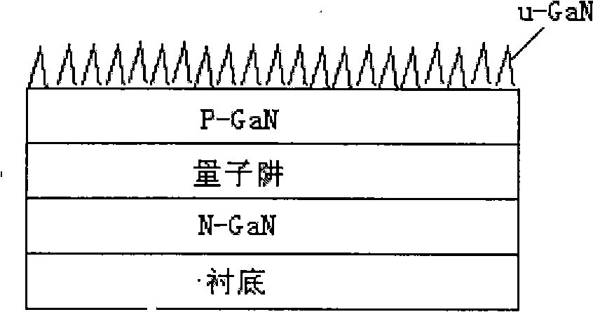
[0017] First, the N-GaN layer, the quantum well layer, the P-GaN layer, and the undoped roughened GaN layer (u-GaN) are sequentially grown on the semiconductor substrate, such as Figure 2A As shown, the non-doped roughened GaN layer is in the shape of a cone, and the apex angle of each formed cone can be adjusted by controlling the growth conditions to make it more pointed. In this embodiment, various layers are formed on the semiconductor substrate by using continuous growth. In addition, the material of the...


PUM


Abstract

The invention discloses a preparation method capable of roughening the surface of a p-GaN layer of an LED. First, an N-GaN layer, a quantum well layer, a P-GaN layer and an undoped roughening GaN layer grow on a semi-conductor substrate in sequence, second, ICP or ion dry etching are adopted to etch the undoped roughening GaN layer so that the shape of the roughening surface of the undoped roughening GaN layer is transmitted to the p-GaN layer, thus causing the surface of the P-GaN layer to be roughened. Compared with the prior art, the preparation method is easy to operate and has better roughening effect.

Description

technical field [0001] The invention relates to a roughening process, in particular to a manufacturing method capable of roughening the surface of a P-GaN layer of an LED. Background technique [0002] The new generation of semiconductor materials represented by GaN has attracted widespread attention due to its wide direct bandgap (Eg=3.4eV), high thermal conductivity, high hardness, high chemical stability, low dielectric constant, and radiation resistance. It has great application potential in the fields of solid-state lighting, solid-state lasers, optical information storage, and ultraviolet detectors. The common LED chip manufacturing process is to first form a stacked structure of N-GaN layer, quantum well layer, and P-GaN layer on a sapphire substrate, and then make each electrode on the stacked structure, such as N electrode, P electrodes etc. However, it is difficult for the light-emitting diodes produced by the existing technology to have a major breakthrough in l...

Claims


Application Information

Patent Timeline
Patent Type & Authority Applications(China)
IPC IPC(8): H01L33/00
Inventor 郝茂盛周健华张楠陈诚潘尧波
Owner EPILIGHT TECH
Why Eureka
Try Eureka