Power trench MOSFET having SiGe/Si channel structure

A channel region, trench gate technology, applied in sustainable manufacturing/processing, climate sustainability, semiconductor devices, etc., can solve problems such as limiting device performance, limiting power efficiency, limiting converter efficiency, etc., to improve device performance. characteristics, the effect of reducing parasitic gate resistance

Inactive Publication Date: 2009-08-19
FAIRCHILD SEMICON CORP
View PDF1 Cites 6 Cited by
  • Summary
  • Abstract
  • Description
  • Claims
  • Application Information

AI Technical Summary

Problems solved by technology

While silicide can be used to reduce this series resistance, the effectiveness of the process is limited by the physical structure of these transist...

Method used


Image

  • Power trench MOSFET having SiGe/Si channel structure
  • Power trench MOSFET having SiGe/Si channel structure
  • Power trench MOSFET having SiGe/Si channel structure

Examples


Embodiment Construction

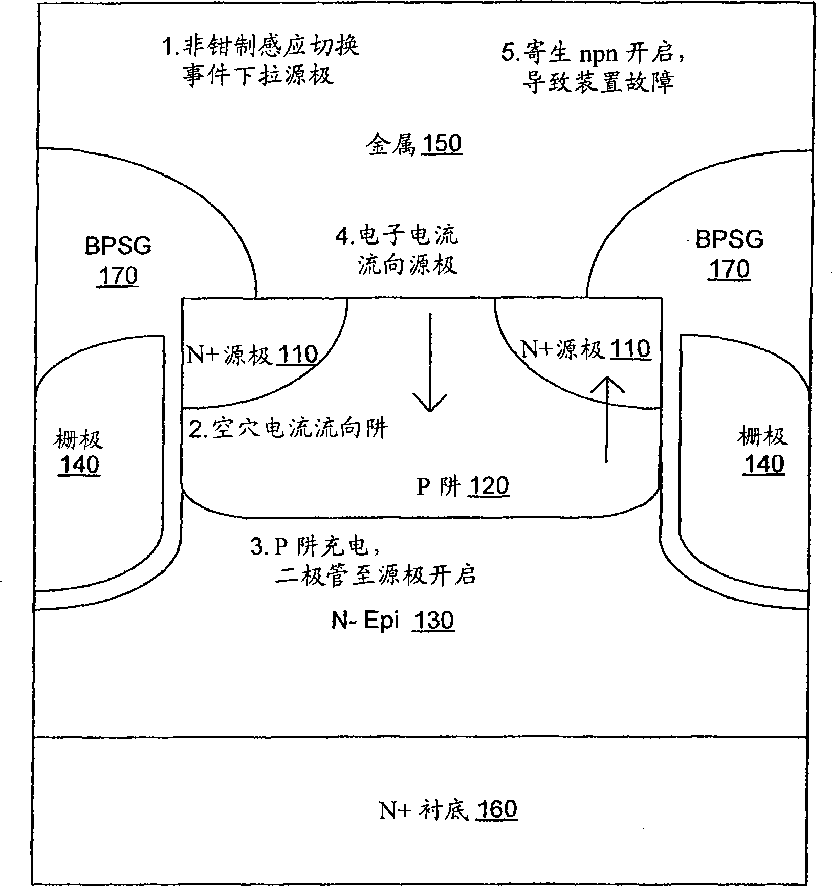
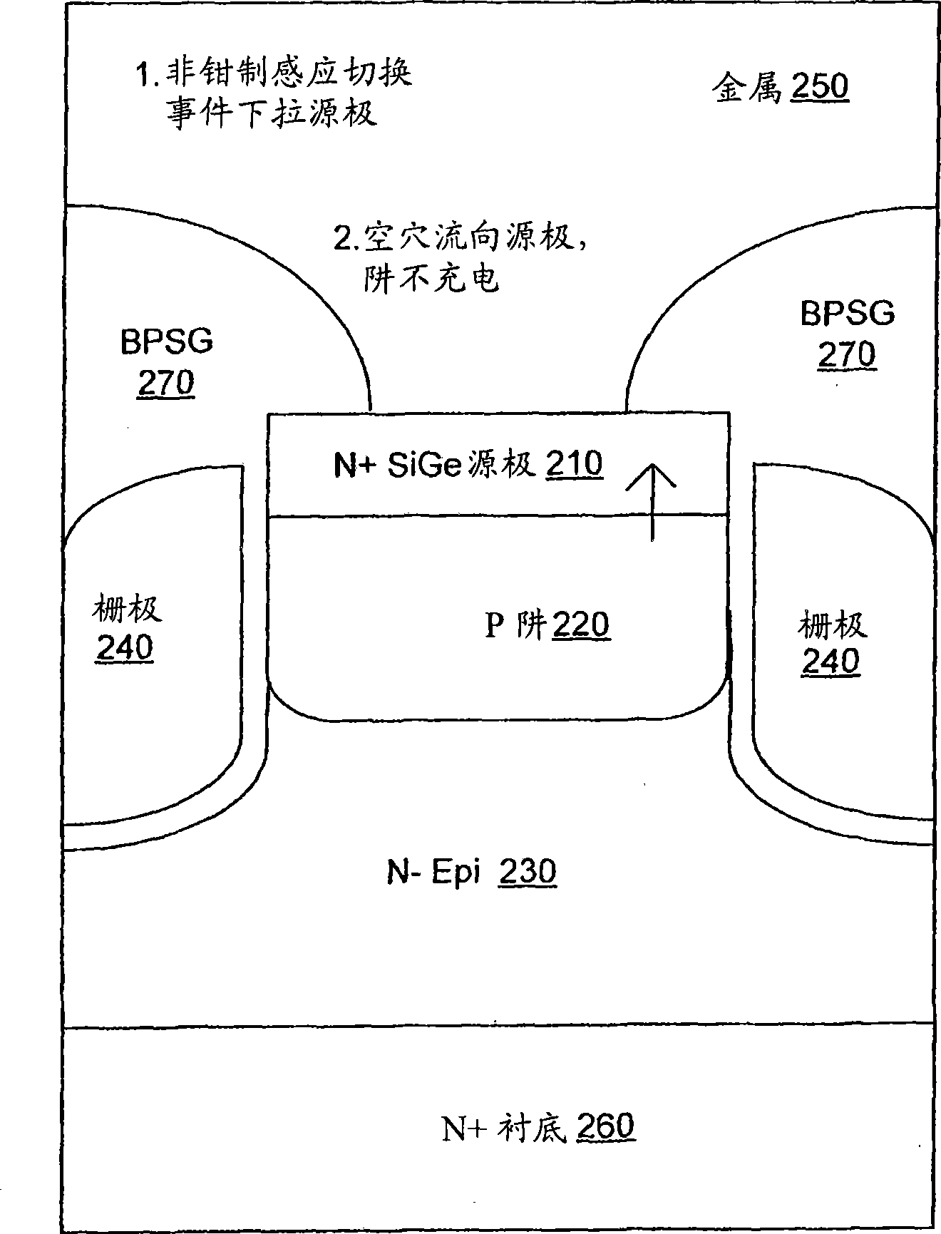
[0039] figure 1 It is a cross-sectional view of an n-channel trench gate power MOSFET improved by combining the embodiment of the present invention. The device includes an n-type source region 110 , a body formed by a p-well 120 , an n-type drain region 130 , a substrate 160 , a gate 140 , and a metal contact 150 .

[0040] Parasitic npn bipolar transistors are inherent in this structure. Specifically, the emitter of the parasitic device is the source region 110 , the base thereof is the body or well region 120 , while the collector of the parasitic device corresponds to the epi region 130 . If this parasitic transistor is biased into its active-forward mode of operation, destructive failure will occur. This can occur, for example, during avalanche breakdown caused by an unclamped inductive switching (UIS) event. Holes generated by impact ionization may flow through the base formed by the P-well 120, causing an ohmic voltage drop. If this voltage drop exceeds about 0.6V, t...


PUM


Abstract

Devices, methods, and processes that improve immunity to transient voltages and reduce parasitic impedances. Immunity to unclamped inductive switching events is improved. For example, a trench-gated power MOSFET device having a SiGe source is provided, where the SiGe source reduces parasitic npn transistor gain by reducing hole current in the body or well region, thereby decreasing the likelihood of a latch-up condition. A trench-gated power MOSFET device having a SiGe body or well region is also provided. A SiGe body reduces hole current when the body diode is turned on, thereby reducing reverse recovery power losses. Other device characteristics are also improved. For example, parasitic gate impedance can reduced through the use of a poly SiGe gate. Also, channel resistance can be reduced through the use of a SiGe layer near the device's gate and a thick oxide region can be formed under the trench gate to reduce gate-to-drain capacitance.

Description

[0001] This application is a continuation-in-part of U.S. Patent Application No. 11 / 245995, filed October 7, 2005 and claims U.S. Provisional Application Nos. 60 / 617167, 60 / 617464, Priority Nos. 60 / 617463, and 60 / 617168, the entire contents of which are hereby incorporated by reference. technical field [0002] The present invention relates generally to power transistors, and more particularly to metal oxide semiconductor gate (MOS gate) power transistors having silicon germanium (SiGe) sources, wells, channels, polysilicon germanium gates, or combinations thereof. Background technique [0003] Trench gate power MOSFET devices are a popular choice for many demanding applications such as DC-DC converters. These applications can be very demanding, putting a lot of strain on these transistors. For example, sinking and sinking large currents into inductive loads can result in large voltage transients at the terminals of one or more devices. In particular, large voltage excursi...

Claims


Application Information

Patent Timeline
IPC IPC(8): H01L29/80
CPCH01L29/66734H01L29/7813H01L29/7782H01L29/4933H01L29/1054H01L29/165H01L29/49Y02P70/50H01L29/80
Inventor 朴赞毫王琦
Owner FAIRCHILD SEMICON CORP
Why Eureka
Try Eureka