Semiconductor component

一种半导体、元件的技术,应用在静态随机存储器晶胞结构及其制造领域,能够解决静态随机存储器晶胞制造合格率下降等问题,达到缩减尺寸、提升性能、提高制造合格率的效果

Active Publication Date: 2009-09-23
TAIWAN SEMICON MFG CO LTD
View PDF0 Cites 3 Cited by
  • Summary
  • Abstract
  • Description
  • Claims
  • Application Information

AI Technical Summary

Problems solved by technology

This problem may also lead to a decline in the manufacturing yield of SRAM cells

Method used


Image

  • Semiconductor component
  • Semiconductor component
  • Semiconductor component

Examples


Embodiment Construction

[0062] The manufacture and application of the preferred embodiments are discussed in detail below. It should be appreciated, however, that the present invention provides many applicable innovative concepts that can be embodied in a wide variety of specific contexts. The specific embodiments discussed are merely illustrative of specific ways to make and use the invention, and do not limit the scope of the invention.

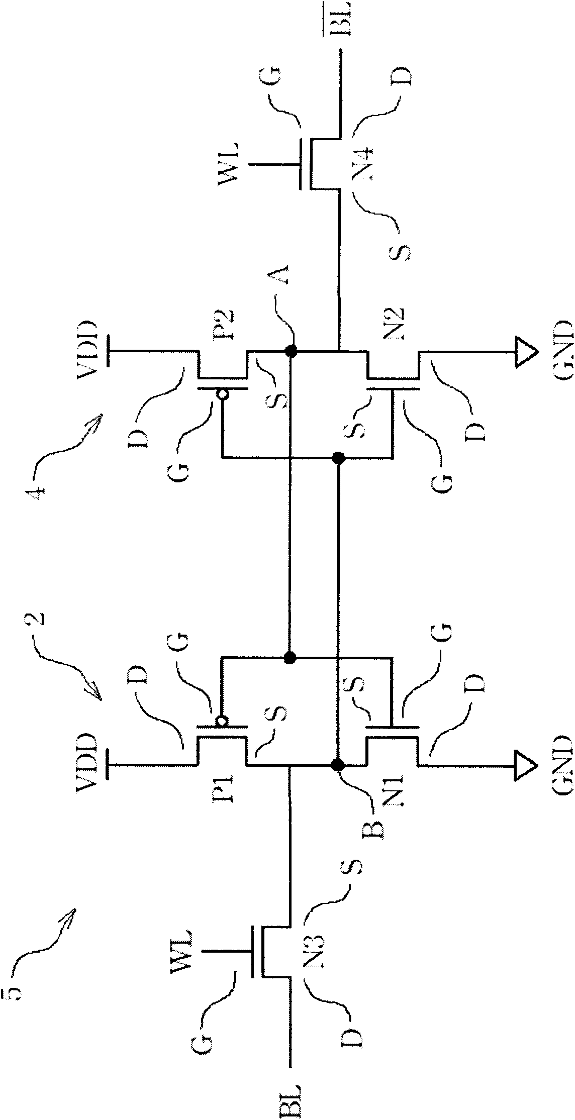
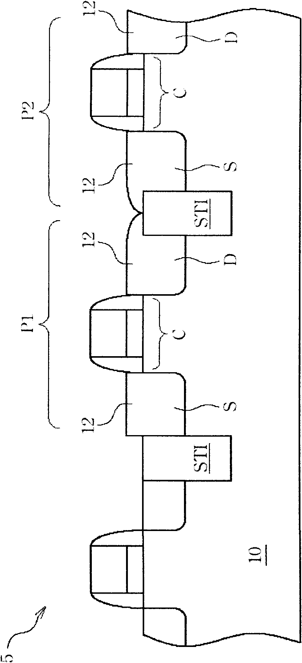
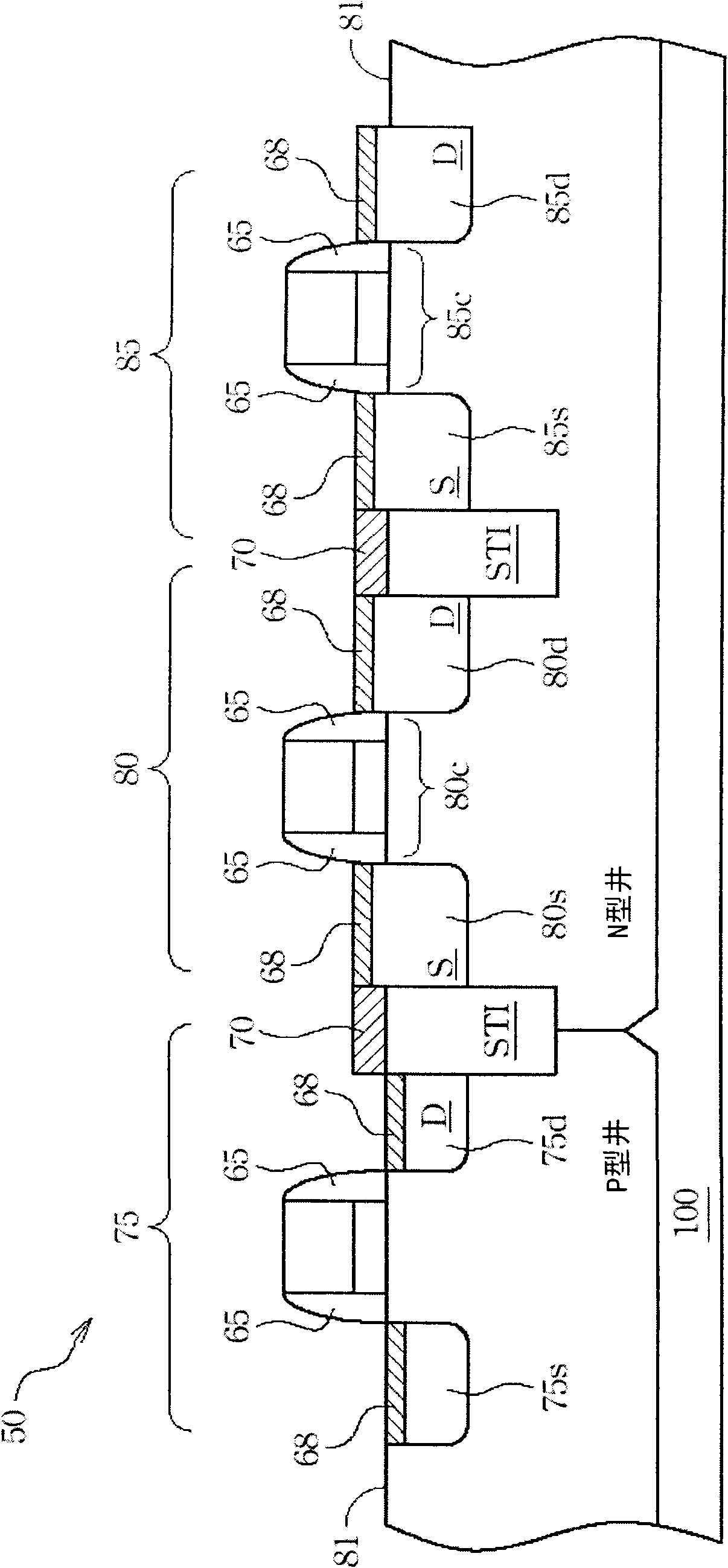
[0063] The present invention will be described in terms of preferred embodiments in a specific context called enhanced SRAM devices and SRAM cell structures and methods of manufacturing the same. The innovative SRAM cell structure includes at least a raised insulating layer on an element isolation region between adjacent PMOS source / drain regions, And the source / drain region at least includes a raised epitaxial silicon germanium (SiGe) layer. The integration of the raised insulating layer on the device isolation region can be fabricated by adding some process st...


PUM


Abstract

The invention relates to a semiconductor element, at least comprising a substrate having an upper surface; the substrate is formed by a first semiconductor material of a first crystallographic lattice constant; a first region at least comprises a first concave portion in the substrate; the first concave portion is filled with a second semiconductor material; the second semiconductor material has a second crystallographic lattice constant; a second region at least comprises a second concave portion in the substrate; the second concave portion is filled with a second semiconductor material; and a separated region is arranged between the first region and the second region; the separated region has a first insulated layer and a second insulated layer; the first insulated layer is extended to the substrate; the second insulated layer is located on the first insulated layer and the upper surface extended on the substrate.

Description

technical field [0001] The present invention generally relates to a semiconductor device, and in particular to a static random access memory (SRAM) device and cell structures of the static random access memory (SRAM) using a strained channel transistor to improve the performance of the transistor and its manufacture method. Background technique [0002] As the trend towards integration of complex electronic systems in integrated circuits (ICs) continues, there is an increasing demand for high-performance memory devices for storing software programs and processed data. As a reliable and proven technology, Static Random Access Memory (SRAM) is a high-performance independent memory element or embedded memory element used in an integrated circuit with a system-on-a-chip (SOC) architecture. Natural selection (Instinctive Choice). The advantages of SRAM compared with other storage devices include fast access speed, low power consumption, high noise margin, and process compatibil...

Claims


Application Information

Patent Timeline
Patent Type & Authority Applications(China)
IPC IPC(8): H01L27/11
CPCH01L27/1104H01L27/11H10B10/00H10B10/12H01L21/823864H01L21/8238
Inventor 庄学理蔡宏智郑光茗梁孟松
Owner TAIWAN SEMICON MFG CO LTD
Why Eureka
Try Eureka