

Thin-film transistor, its manufacturing method, and display
A thin-film transistor and source technology, applied in transistors, semiconductor/solid-state device manufacturing, semiconductor devices, etc., can solve the problems of inability to obtain conduction current, achieve improved carrier mobility, high performance, and suppress leakage current Effect
- Summary
- Abstract
- Description
- Claims
- Application Information
AI Technical Summary
Problems solved by technology
Method used
Image

Examples
no. 1 example
[0038] figure 1 is a cross-sectional view of the thin film transistor for explaining the first embodiment. The thin film transistor 1 shown in the figure is an n-type bottom gate thin film transistor. Strip-shaped gate electrodes 3 formed of, for example, molybdenum are pattern-formed on a substrate 2 made of an insulating substrate such as glass. The gate electrode 3 is not particularly limited, and the material may not be molybdenum as long as the material is a refractory metal that is hardly changed by heat generated when the crystallization process is performed.
[0039] A gate insulating film 4 made of, for example, a silicon oxide film is also formed to cover the gate electrode 3 . The gate insulating film 4 may be formed of a silicon nitride film, a silicon oxynitride film, or a laminated film thereof, other than a silicon oxide film.
[0040] Further, a channel layer 5 made of, for example, amorphous silicon is pattern-formed on this gate insulating film 4 in a sta...
no. 2 example
[0084] (thin film transistor)
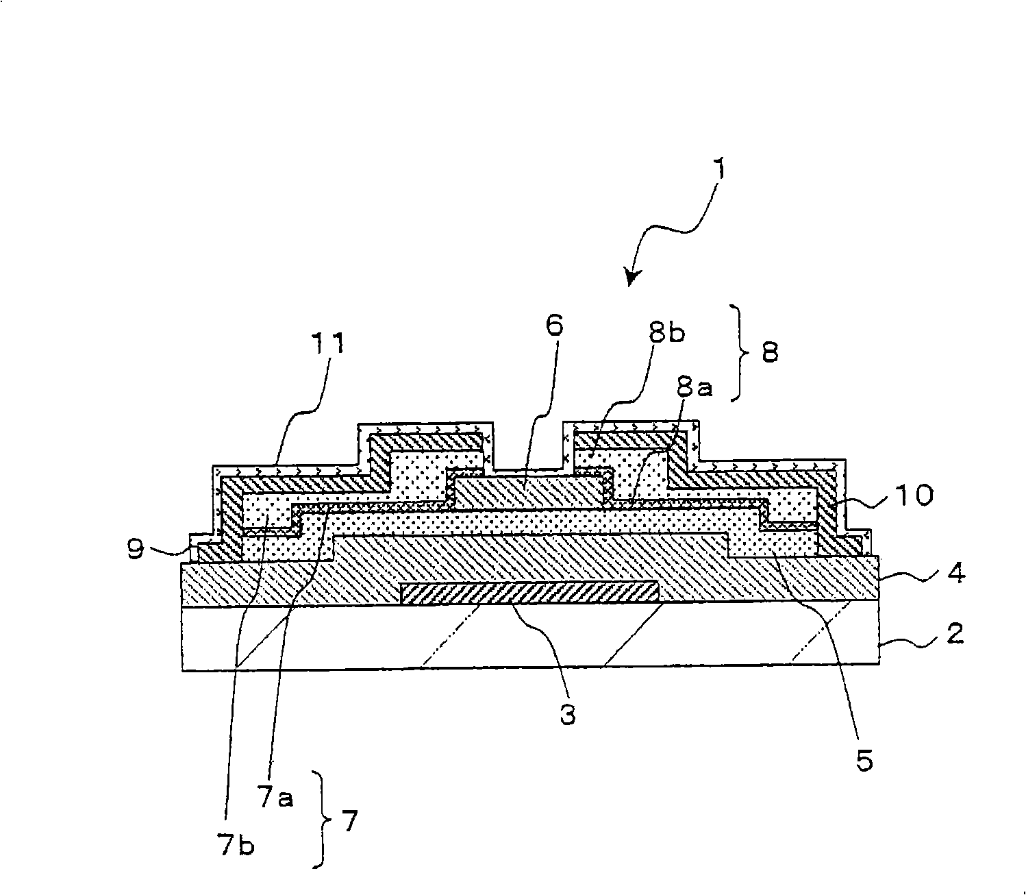
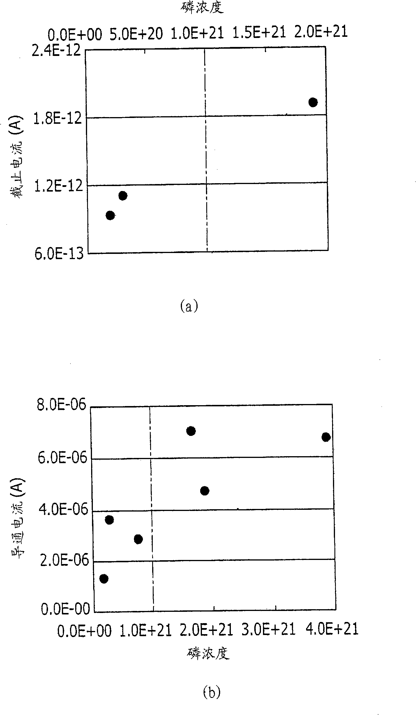
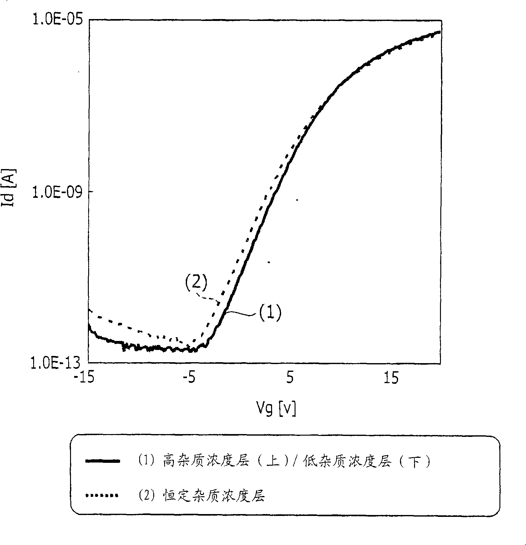
[0085] Figure 9 is a cross-sectional view of a thin film transistor for explaining the second embodiment. The thin film transistor 1' shown in this figure is a top gate type thin film transistor, and a source layer 7 and a drain layer 8 are provided by being laminated on a source electrode 9 and a drain electrode 10 patterned on a substrate 2 . Furthermore, as a characteristic structure in the present invention, source / drain layers 7 and 8 contain impurities with a concentration gradient such that the concentration becomes lower toward channel layer 5 . Specifically, the source layer 7 has a two-layer structure consisting of the second silicon layer 7b covering the source electrode 9 and the first silicon layer 7a on the second silicon layer, and the drain layer 8 has a silicon layer covering the drain electrode 10. A two-layer structure composed of the second silicon layer 8b and the first silicon layer 8a on the second silicon layer. Ther...
PUM
 Abstract
Description
Claims
Application Information