

Semiconductor tube of hyperconjugation longitudinal double diffusion metal oxide with N channels
A vertical double-diffusion, semiconductor tube technology, used in semiconductor devices, electrical components, circuits, etc., can solve the problems of small drift layer thickness, no longer suitable for super junction structure devices, and high drift region concentration, to increase area, improve Reliability and stability, the effect of improving the working current
- Summary
- Abstract
- Description
- Claims
- Application Information
AI Technical Summary
Problems solved by technology
Method used
Image

Examples
Embodiment Construction
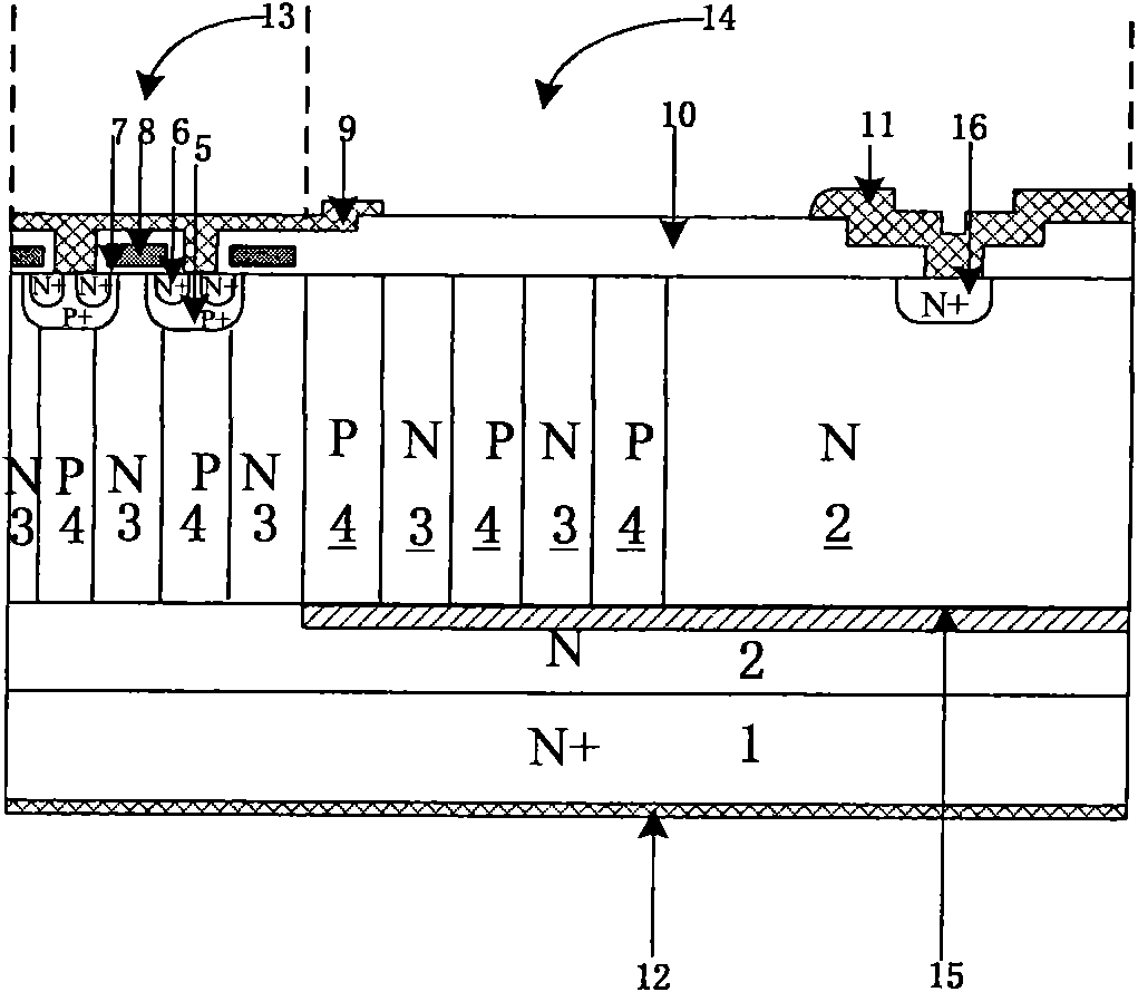
[0015] An N-channel superjunction vertical double-diffused metal oxide semiconductor tube, comprising: an N-type doped silicon substrate 1 serving as a drain region, an N-type doped silicon epitaxial layer 2, a primary cell region 13, and a primary cell 13 Around the terminal region 14, the N-type doped silicon epitaxial layer 2 is arranged on the N-type doped silicon substrate 1, and the original cell region 13 and the terminal region 14 are arranged on the N-type doped silicon epitaxial layer 2, and the terminal Region 14 includes a first super junction structure and an N-type silicon-doped semiconductor region 2 , in the N-type silicon-doped semiconductor region 2 An N-type heavily doped semiconductor region 16 is provided in the middle, and the first superjunction structure and the N-type silicon-doped semiconductor region 2 A field oxide layer 10 is arranged on it, a metal layer 11 is connected on the N-type heavily doped semiconductor region 16 , and a buried oxide laye...
PUM
 Abstract
Description
Claims
Application Information