Method for preparing front electrodes of solar cells

A technology for solar cells and front electrodes, which is applied in the manufacture of circuits, electrical components, and final products. It can solve the problems of very high screen printing accuracy, no advantages, and reduced recombination, so as to avoid alignment problems and achieve good aspect ratios. , Reduce the effect of shading area

Inactive Publication Date: 2009-10-21
INST OF ELECTRICAL ENG CHINESE ACAD OF SCI
View PDF2 Cites 40 Cited by
  • Summary
  • Abstract
  • Description
  • Claims
  • Application Information

AI Technical Summary

Problems solved by technology

Chinese invention patent application 200810219091.2 proposes a front electrode of a bridge structure. Although it also has the characteristics of point contact, two kinds of pastes are used for two silk screen printings, requiring that the two silk screens must be completely overlapped, otherwise it is easy to cause grid breakage, so for Screen printing accuracy requirements are very high
Moreover, the electrodes prepared by this method are not thinner than conventional ones, so there are no advantages in reducing light shading and reducing recombination

Method used


Image

  • Method for preparing front electrodes of solar cells
  • Method for preparing front electrodes of solar cells
  • Method for preparing front electrodes of solar cells

Examples


Embodiment 1

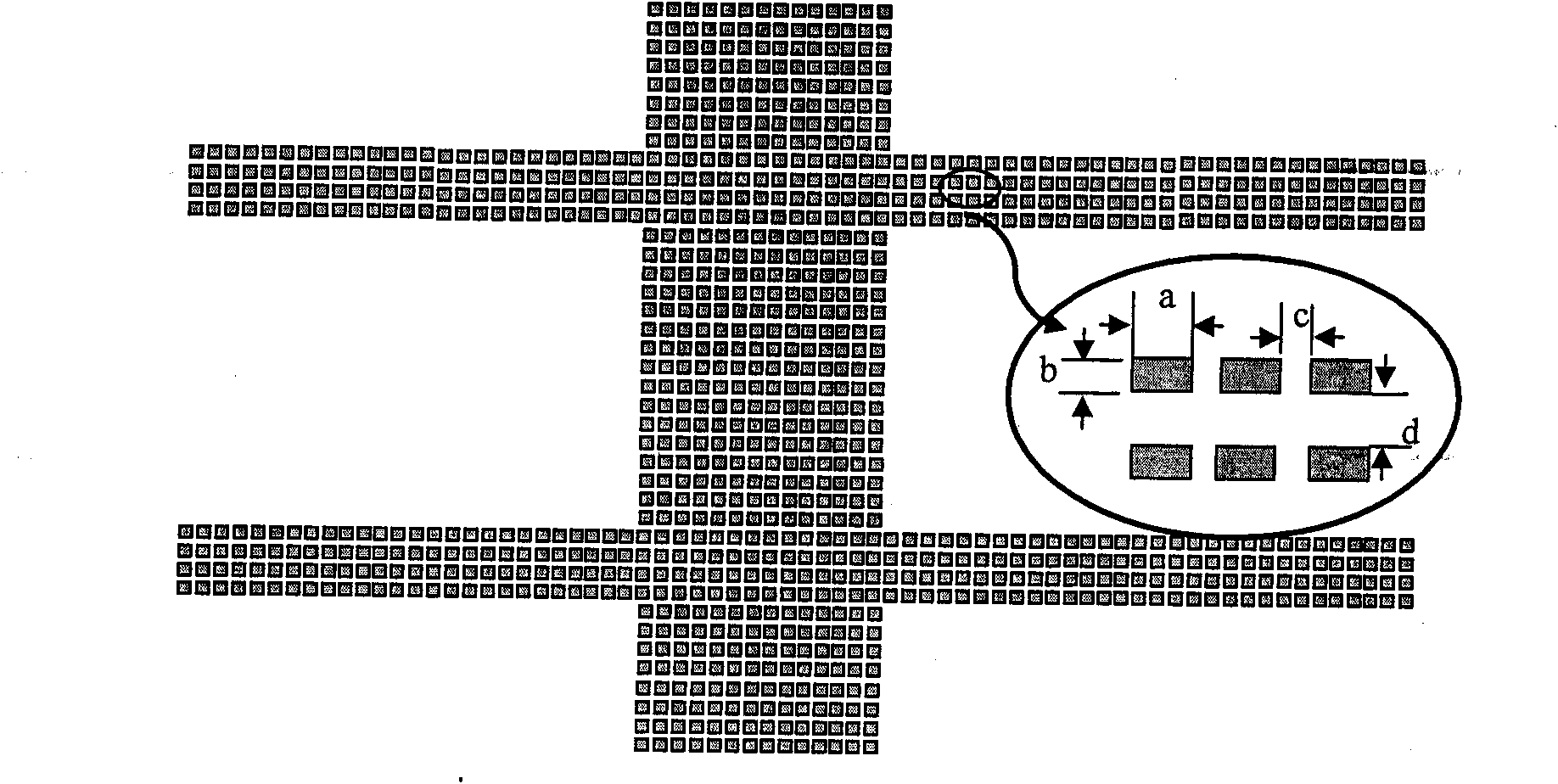
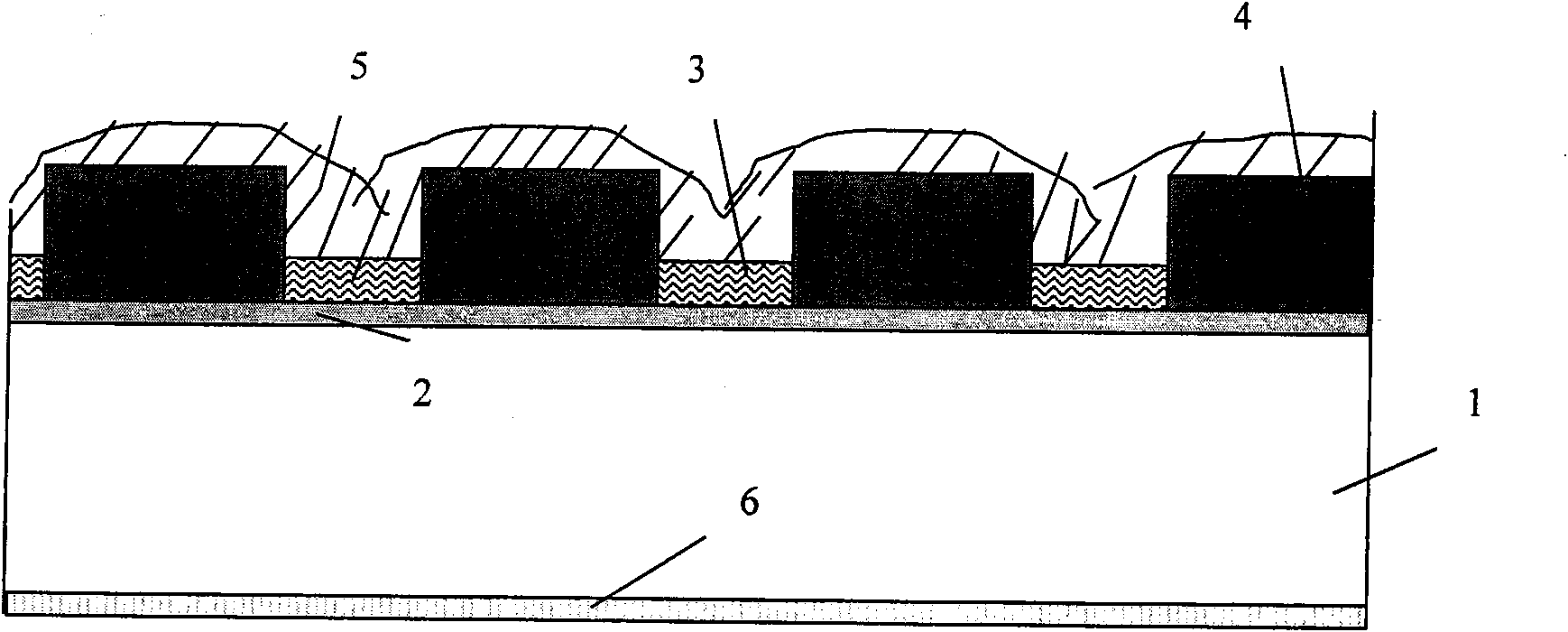
[0034] Example 1: After P-type silicon substrate (1) is cleaned and textured by conventional industrial cleaning methods, POCl is diffused at 850°C 3 The liquid source was used for 30 minutes to obtain an N-type emitter (2) of about 40Ω / □. Deposit a layer of SiN of about 90nm on the emitter with PECVD equipment x After the thin film is used as the dielectric film (3), screen-print aluminum paste on the side of the silicon substrate (1) without the dielectric film (3) as the back electrode (6), and then screen-print dot-shaped discontinuous Ag on the dielectric film by a screen printing machine. Metal paste (4), dot electrode patterns are determined by the screen used. The length a of the point electrodes is 10 μm, the width b is 60 μm, the length of the horizontal spacing c of the point electrodes is 10 μm, and the length of the vertical spacing d is 0 μm. Putting the silicon substrate (1) which has completed the silk screen printing process into a sintering furnace for sint...

Embodiment 2

[0035] Example 2: After P-type silicon substrate (1) is cleaned and textured by conventional industrial cleaning methods, POCl is diffused at 850°C 3 The liquid source is used for 30 minutes to obtain an N-type emitter (2) of about 40Ω / □. Then prepare the dielectric film (3), the steps are as follows: oxidize at 860°C for 10 minutes to obtain a layer of SiO with a thickness of about 10nm 2 thin film, followed by APCVD on SiO 2 Deposit a layer of 80nm TiO on the film 2 Thin film, complete the preparation of the dielectric film (3). On the side of the P-type silicon substrate (1) without the dielectric film (3), the aluminum paste is screen-printed to form the back electrode (6) and then the dot-shaped discontinuous Ag metal paste is screen-printed on the dielectric film (3) through a screen printing machine ( 4), the dot electrode pattern is determined by the screen. Wherein the length a of the dot electrodes is 10 μm, the width b is 10 μm, the horizontal spacing length c o...

Embodiment 3

[0036] Example 3, P-type silicon substrate (1) was cleaned and textured by conventional industrial cleaning methods, and POCl was diffused at 850°C 3 The liquid source is used for 30 minutes to obtain an N-type emitter (2) of about 40Ω / □. Then deposit a layer of SiN of about 90nm on the emitter (2) by PECVD x After the thin film is used as the dielectric film (3), screen-print aluminum paste on the side of the silicon substrate (1) without the dielectric film (3) to form the back electrode (6), and screen-print dots on the dielectric film (3) by a screen printing machine. Discontinuous Ag electrode paste (4), dot electrode pattern is determined by the screen used. The length a of the point electrodes is 100 μm, the width b is 20 μm, the length of the horizontal interval c of the point electrodes is 100 μm, and the length of the vertical interval d is 0 μm. The silicon substrate (1) which has completed the silk screen printing process is put into a sintering furnace for sinte...


PUM

PropertyMeasurementUnit
lengthaaaaaaaaaa
widthaaaaaaaaaa
widthaaaaaaaaaa

Abstract

The invention relates to a method for preparing front electrodes of solar cells, which comprises the following steps: firstly preparing discontinuous dot electrodes; and then connecting the dot electrodes by electroplating technology to realize that the electrodes collect and transport current but dielectric films still exist between the dot electrodes to have the function of passivation. The discontinuous dot electrodes are prepared by photoetching, evaporation and dissection methods, or firstly printed by silkprint, stencil printing or ink jet printing and then prepared by a sintering method. The electroplating is photoinductive electroplating or chemical plating. The dot electrodes effectively reduce surface recombination; and the adopted electroplating technology not only simply and accurately realizes the connection of the dot electrodes, but also effectively reduces the width of grid lines, namely reduces electrode shading areas and further reduces the surface recombination so as to contribute to improving battery efficiency.

Description

technical field [0001] The invention relates to a method for preparing a front electrode of a solar cell. Background technique [0002] At present, the industrialization technology of crystalline silicon solar cells is very mature. In recent years, with the increase of market demand, the scale of industrialization has shown a momentum of rapid expansion. However, compared with conventional energy sources, its relatively high cost and low efficiency restrict the development of solar cells. Extensive research has been conducted on how to reduce battery cost and improve battery efficiency. [0003] Among the factors affecting efficiency, the design of the front electrode of the cell is also a key factor, because the electrode is on the incident light side of the cell and is in direct contact with the emitter of the underlying layer. Therefore, on the one hand, the area of ​​the front electrode should be as small as possible, which can reduce the shielding of the incident ligh...

Claims


Application Information

Patent Timeline
Patent Type & Authority Applications(China)
IPC IPC(8): H01L31/18H01L31/0224C25D5/00
CPCY02P70/50
Inventor 李海玲王文静周春兰赵雷刁宏伟
Owner INST OF ELECTRICAL ENG CHINESE ACAD OF SCI
Why Eureka
Try Eureka