Photosensitive element

A photosensitive, photosensitive resin technology, applied in electrical components, optics, optomechanical equipment, etc., can solve the problems of polluting optical tools, exposure of photosensitive layer, photosensitivity decline, etc., and achieve excellent resolution and excellent peeling effect

Active Publication Date: 2009-10-21
RESONAC CORPORATION
View PDF5 Cites 0 Cited by
  • Summary
  • Abstract
  • Description
  • Claims
  • Application Information

AI Technical Summary

Problems solved by technology

However, since the photosensitive layer usually has a certain degree of adhesion, when the optical tool is directly attached to the photosensitive layer for exposure, it is not easy to remove the attached optical tool.
In addition, the photosensitive layer will pollute the optical tool, and peeling off the support film will cause the photosensitive layer to be exposed to oxygen in the atmosphere, which will easily lead to a decrease in photosensitivity

Method used


Image

  • Photosensitive element
  • Photosensitive element
  • Photosensitive element

Examples


Embodiment 1

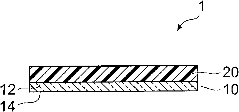
[0137] As a supporting film, a polyethylene terephthalate (hereinafter referred to as "PET") film (manufactured by Toyobo Co., Ltd., trade name "A-1517", thickness 16 μm) was prepared. Next, the above-prepared photosensitive resin composition containing the binder polymer (I) was coated on the PET film to make the thickness uniform, and dried with a hot air convection dryer at 100° C. for 2 minutes to remove the solvent to form a photosensitive layer. After drying, the photosensitive layer was covered with a polyethylene film (manufactured by Tamapoly, trade name "NF-15", thickness 20 μm) as a protective film to obtain a photosensitive element. In addition, the thickness of the photosensitive layer after drying was 25 μm.

Embodiment 2

[0139] A photosensitive element was obtained in the same manner as in Example 1 except that the photosensitive resin composition containing the binder polymer (II) was used instead of the photosensitive resin composition containing the binder polymer (I). . The thickness of the photosensitive layer after drying was 25 μm.


PUM

PropertyMeasurementUnit
acid valueaaaaaaaaaa
thicknessaaaaaaaaaa
hazeaaaaaaaaaa

Abstract

An photosensitive element comprising: a substrate film (10) which has a haze of 1.0% or less and has a surface resistance of 10 O or less on its second main surface (14) opposed to a first main surface (12) thereof; and a layer (20) which comprises a photosensitive resin composition and contains a binder polymer comprising a compound represented by the general formula (I) and (meth)acrylic acid as monomer units, a photopolymerizable compound, and a photopolymerization initiator. H2C=CR-COOR (I) wherein R represents a hydrogen atom or a methyl group; and R represents an alkyl group having 3 to 7 carbon atoms.

Description

technical field [0001] The present invention relates to a photosensitive element. Background technique [0002] Conventionally, in the field of manufacturing printed circuit boards, as a resist material for etching, plating, etc., a layer composed of a photosensitive resin composition (hereinafter referred to as "photosensitive layer"), a support film, and a protective film The photosensitive element constituted has been widely used. A printed circuit board is manufactured, for example, in the following manner. First, the protective film of the photosensitive element is peeled off from the photosensitive layer, and then the photosensitive layer is laminated on the conductive film of the circuit-forming substrate. Next, pattern exposure is performed on the photosensitive layer, and the unexposed portion is removed with a developer to form a resist pattern. Based on this resist pattern, a conductive film is then patterned to form a printed circuit board. [0003] As a deve...

Claims


Application Information

Patent Timeline
Patent Type & Authority Applications(China)
IPC IPC(8): G03F7/004G03F7/033H05K3/00
CPCG03F7/033G03F7/004G03F7/0045G03F7/09
Inventor 久保田雅夫
Owner RESONAC CORPORATION
Why Eureka
Try Eureka