Semiconductor device, n-type MOS transistor and manufacturing method thereof
A technology for MOS transistors and manufacturing methods, which is applied in the field of n-type MOS transistors and their manufacturing, and semiconductor devices, and can solve problems such as insufficient suppression of hot carrier injection effects
- Summary
- Abstract
- Description
- Claims
- Application Information
AI Technical Summary
Problems solved by technology
Method used
Image

Examples
Embodiment Construction
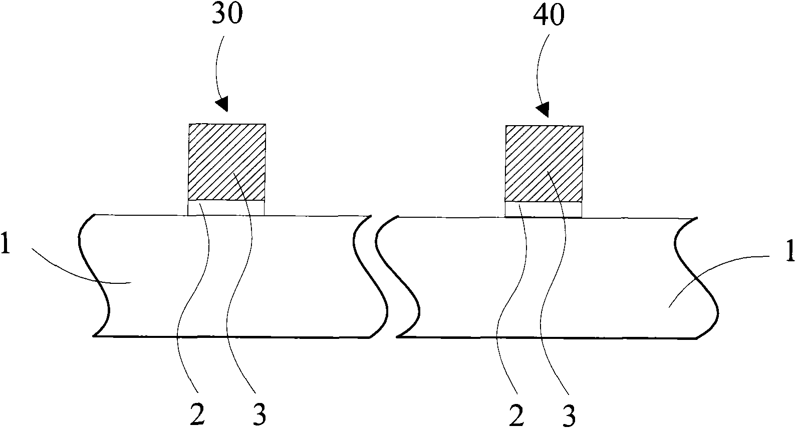
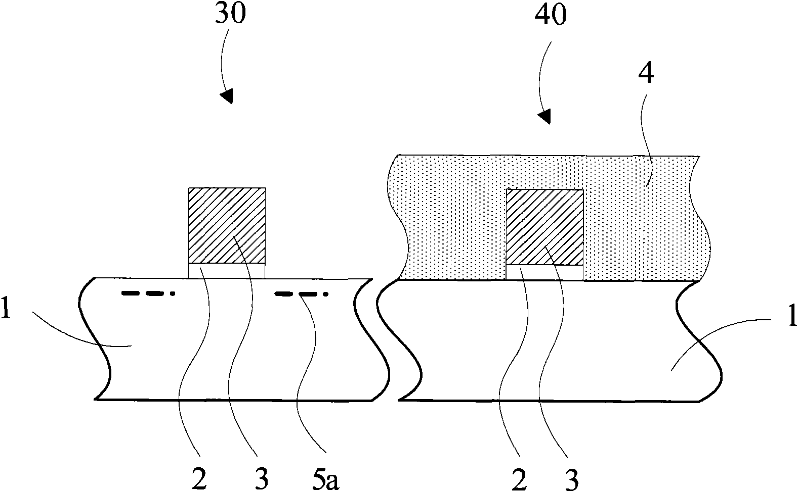
[0035] In the present invention, a fluorine ion implantation region is formed on the surface of the semiconductor substrate above the low-doped source / drain region of the n-type MOS transistor region in the high-voltage device region, and the fluorine ion in the fluorine ion implantation region forms fluorine with silicon in the semiconductor substrate. The silicon group prevents the formation of charge traps and prevents the low-doped source / drain region from accumulating charges under an applied voltage to form a hot carrier effect.
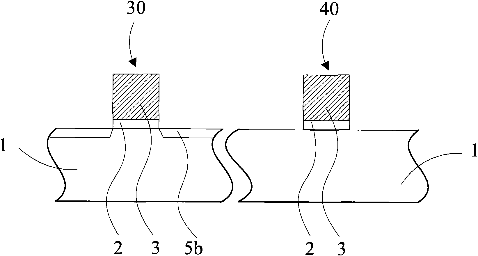
[0036] The present invention performs rapid thermal annealing after the low-doped ion implantation in the n-type MOS transistor area of the high-voltage device area. While activating impurities and eliminating defects generated by ion implantation, the TED effect and self-thermal diffusion can be used to make the junction more compact. In order to gradually change, thereby further reducing the surface electric field of the drain channel, and a...
PUM
 Abstract
Description
Claims
Application Information