Polysilicon membrane forming method and polysilicon gate forming method

A polysilicon film and polysilicon layer technology, which is applied in the directions of polysilicon material growth, chemical instruments and methods, crystal growth, etc., can solve the problem that the polysilicon film cannot take into account the flatness and interface quality, etc., so as to improve the physical and electrical characteristics, Improved formation quality, improved grain size effect

Inactive Publication Date: 2009-11-11
SEMICONDUCTOR MANUFACTURING INTERNATIONAL (BEIJING) CORP
View PDF1 Cites 5 Cited by
  • Summary
  • Abstract
  • Description
  • Claims
  • Application Information

AI Technical Summary

Problems solved by technology

[0013] The invention provides a method for forming a polysilicon thin film and a polysilicon grid, so as to improve the phenomenon that the existing polysilicon thin film formation method cannot meet the requirements of flatness and interface quality, and improve the formation quality of the polysilicon grid

Method used


Image

  • Polysilicon membrane forming method and polysilicon gate forming method
  • Polysilicon membrane forming method and polysilicon gate forming method
  • Polysilicon membrane forming method and polysilicon gate forming method

Examples


no. 1 example

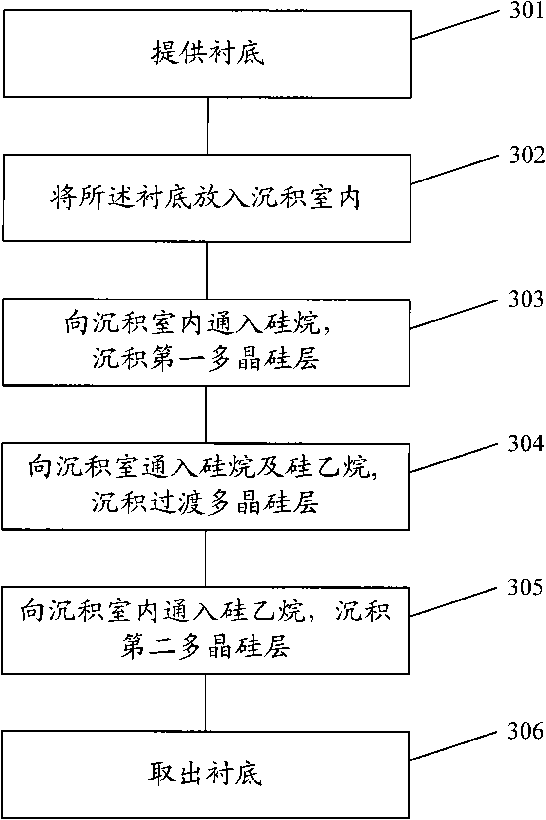
[0069] The first embodiment of the present invention introduces a new method for forming a polysilicon film, image 3 It is a flow chart of the method for forming a polysilicon thin film in the first embodiment of the present invention, Figure 4 to Figure 6 In order to illustrate the device cross-sectional view of the method for forming a polysilicon film in the first embodiment of the present invention, the following is combined Figure 3 to Figure 6 The first embodiment of the present invention will be described in detail.

[0070] Step 301: Provide a substrate.

[0071] The substrate in this embodiment can be a simple silicon substrate, or a substrate with a certain structure formed, for example, a silicon oxide layer can be formed on the surface of the substrate. In addition, in other embodiments of the present invention, the substrate can also be made of other materials, such as germanium material, gallium arsenide material or silicon carbide material.

[0072] Step 3...

no. 2 example

[0102] The second embodiment of the present invention introduces a new gate forming method, Figure 7 is a flow chart of the gate formation method in the second embodiment of the present invention, Figure 8 to Figure 13 In order to illustrate the device cross-sectional view of the gate forming method in the second embodiment of the present invention, the following is combined with Figure 7 to Figure 13 The second embodiment of the present invention will be described in detail.

[0103] Step 701: providing a substrate on which a gate oxide layer has been formed.

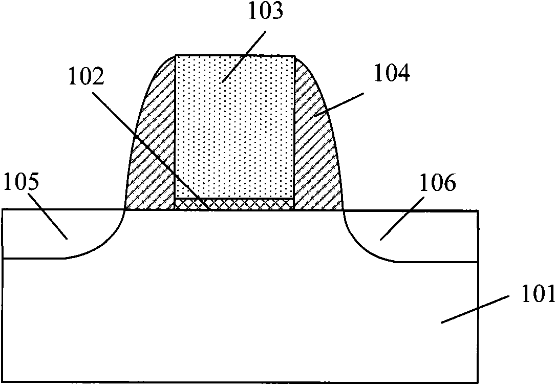
[0104] Figure 8 It is a schematic cross-sectional view of the substrate in the second embodiment of the present invention, as Figure 8 As shown, the substrate in this embodiment includes a silicon substrate 801 and a gate oxide layer 802 thereon. In other embodiments of the present invention, the silicon substrate 801 may also be a substrate of other materials, Such as germanium materials, gallium arsenide mat...


PUM


Abstract

The invention discloses a polysilicon membrane forming method comprising the following steps: providing a substrate; putting the substrate in a settling chamber; leading silane into the settling chamber and settling a first polycrystalline silicon layer on the substrate; leading silane and silicoethane to the settling chamber and settling a transition polycrystalline silicon layer on the first polycrystalline silicon layer; leading silicoethane to the settling chamber and settling a second polycrystalline silicon layer on the transition polycrystalline silicon layer; and taking out the substrate. The invention also correspondingly discloses a method for forming gates by utilizing the polysilicon membrane. The polysilicon membrane formed by the method not only satisfies the requirements of planeness and interface quality, but also enables the transition of each layer of the polysilicon membrane to be more stable, thereby further enhancing the forming quality of the polysilicon membrane.

Description

technical field [0001] The invention relates to the technical field of semiconductor manufacturing, in particular to a method for forming a polysilicon thin film and a polysilicon gate. Background technique [0002] With the rapid development of ultra-large-scale integrated circuits, the integration of chips is getting higher and higher, and the size of components is getting smaller and smaller. The various effects caused by the high density and small size of devices have an increasing impact on the results of semiconductor process manufacturing. Outstanding, new process improvements are often required for small-scale devices. Taking the manufacture of polysilicon gates as an example, when the size of the device is reduced, small-sized devices made with the gate of the original large-sized device tend to have poor gate leakage current performance. The device is no longer suitable and needs to be improved and optimized. [0003] Metal Oxide Semiconductor Transistor (MOSET, ...

Claims


Application Information

Patent Timeline
Patent Type & Authority Applications(China)
IPC IPC(8): H01L21/205H01L21/28H01L21/285H01L21/336C30B28/14
Inventor 何永根
Owner SEMICONDUCTOR MANUFACTURING INTERNATIONAL (BEIJING) CORP
Why Eureka
Try Eureka