Flattening method of interlayer medium layer and forming method of contact hole

A technology of interlayer dielectric layer and planarization method, which is applied in the direction of electrical components, semiconductor/solid-state device manufacturing, circuits, etc., can solve the problems of poor contact hole formation quality and consistency, and achieve the effect of meeting high requirements and high flatness

Inactive Publication Date: 2009-11-11
SEMICONDUCTOR MANUFACTURING INTERNATIONAL (BEIJING) CORP
View PDF0 Cites 15 Cited by
  • Summary
  • Abstract
  • Description
  • Claims
  • Application Information

AI Technical Summary

Problems solved by technology

[0011] The invention provides a method for planarizing an interlayer dielectric layer and a method for forming a contact hole, so as to improve the formation quality of the existing contact hole caused by the poor flatness of the formed interlayer dielectric layer in the wafer and poor consistency

Method used


Image

  • Flattening method of interlayer medium layer and forming method of contact hole
  • Flattening method of interlayer medium layer and forming method of contact hole
  • Flattening method of interlayer medium layer and forming method of contact hole

Examples


no. 1 example

[0064] Figure 5 is a flow chart of the method for planarizing the interlayer dielectric layer in the first embodiment of the present invention, Figure 6 to Figure 9 In order to illustrate the cross-sectional view of the device of the method for planarizing the interlayer dielectric layer in the first embodiment of the present invention, the following is combined with Figure 5 to Figure 9 The first embodiment of the present invention will be described in detail.

[0065] Step 501: Provide a substrate, and the substrate already has a gate structure.

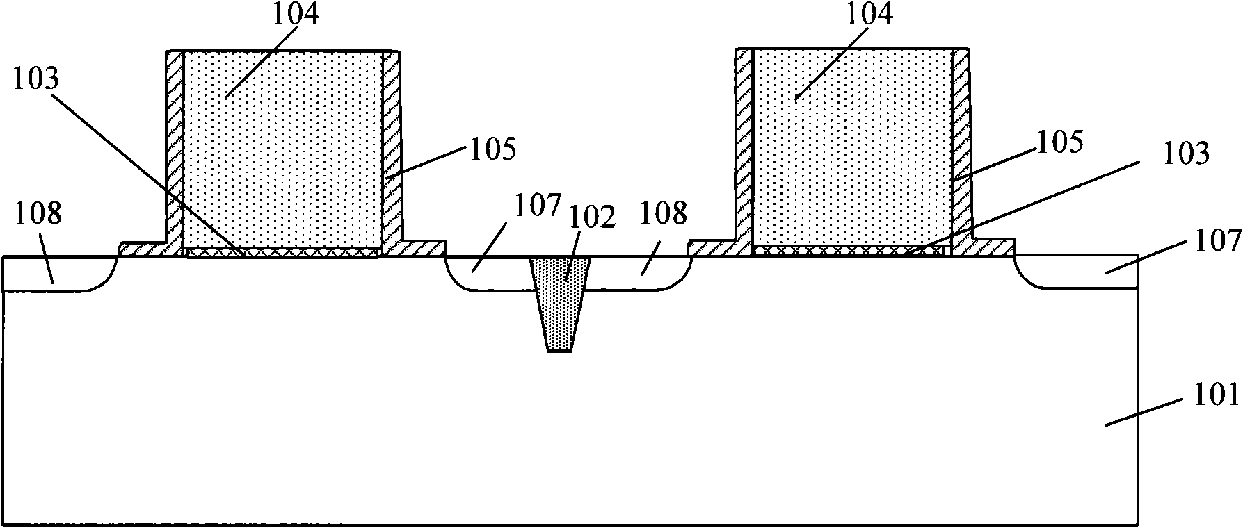
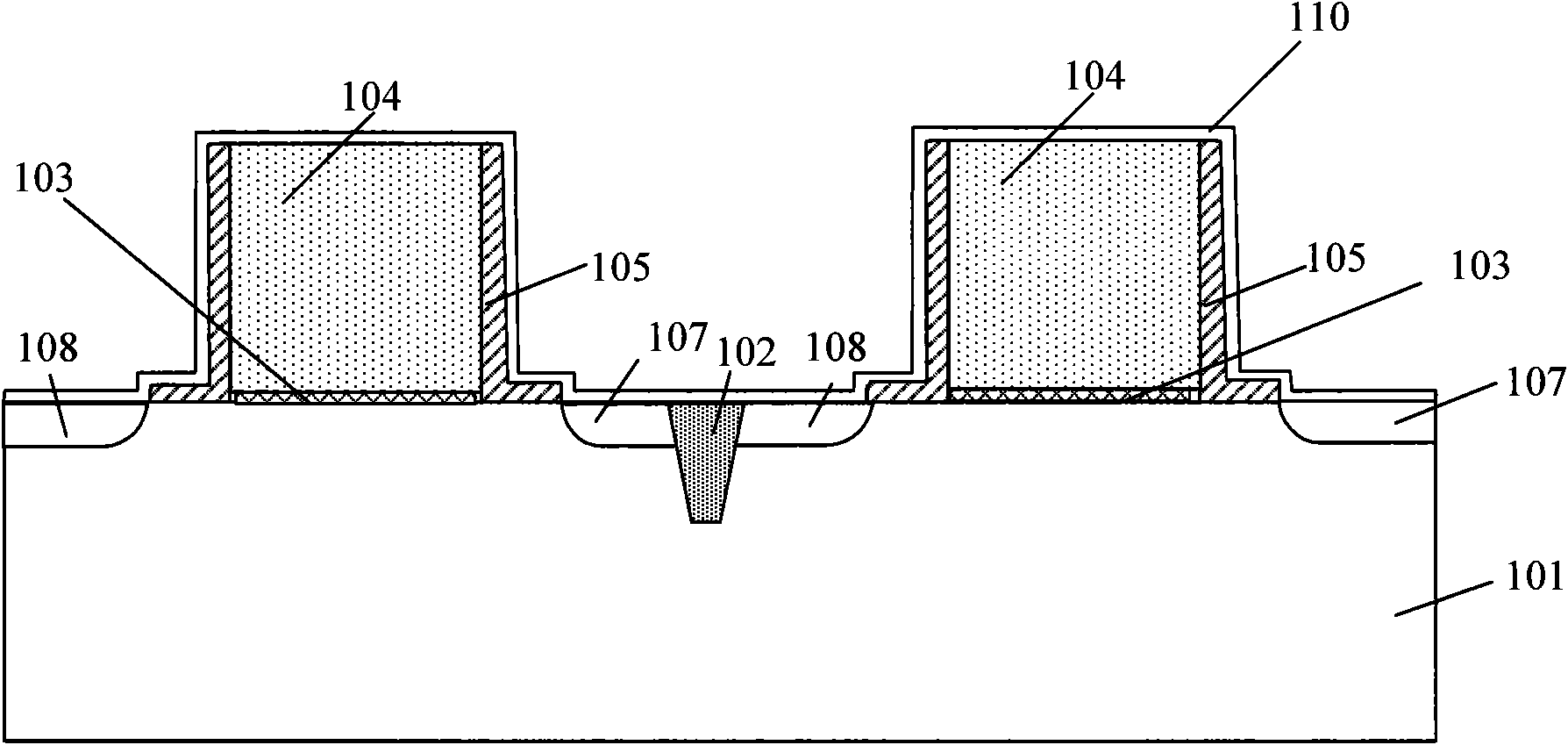
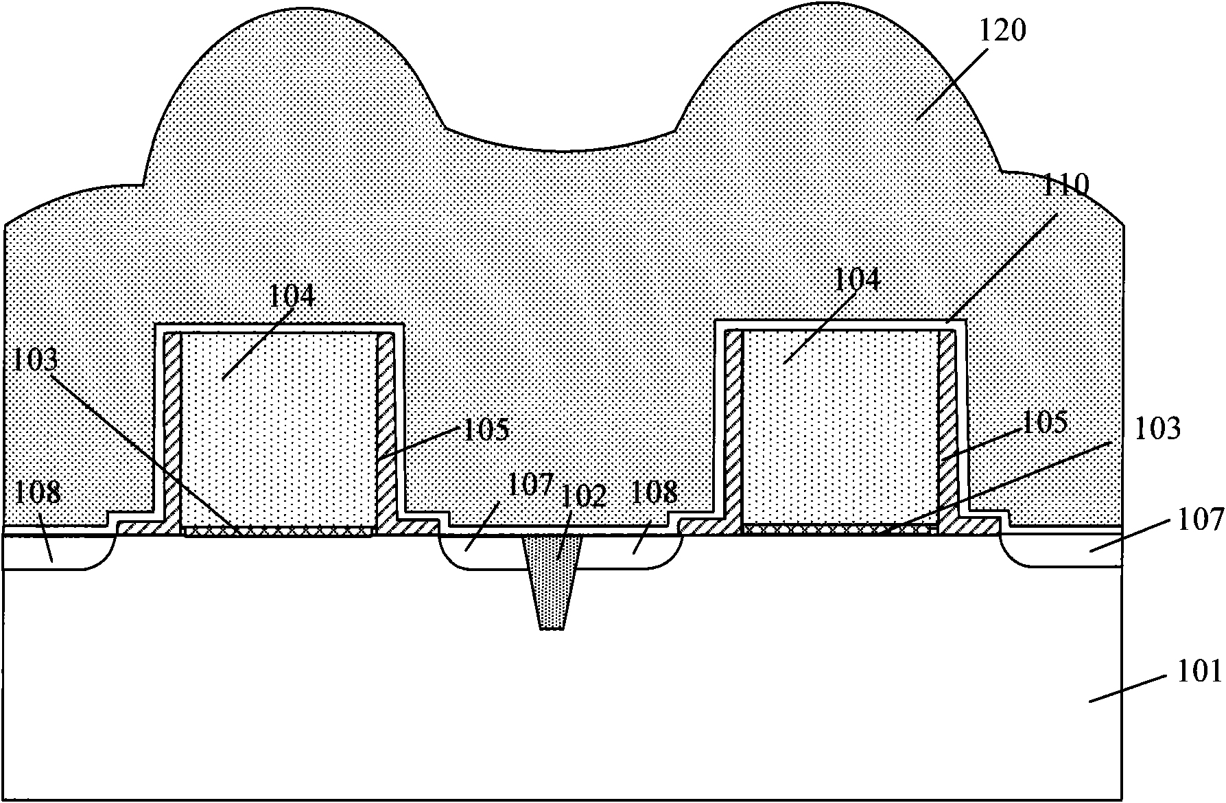
[0066] Figure 6 It is a schematic cross-sectional view of the substrate used in the first embodiment of the present invention, such as Figure 6 As shown, the structure of the substrate is as follows: a gate 604 with a gate oxide layer (GateOxide) 603 at the bottom is formed on a silicon substrate 601, and isolation trenches 602 are formed between each device; A gate sidewall layer 605 is formed on the silicon substrate 601...

no. 2 example

[0087] Figure 10 It is a flowchart of a method for forming a contact hole in the second embodiment of the present invention, Figure 11 to Figure 16 In order to illustrate the cross-sectional view of the device of the method for forming the contact hole of the second embodiment of the present invention, the following is combined with Figure 10 to Figure 16 The second embodiment of the present invention will be described in detail.

[0088] Step 1001: Provide a substrate, and the substrate already has a gate structure.

[0089] Figure 11 It is a schematic cross-sectional view of the substrate used in the second embodiment of the present invention, such as Figure 11 As shown, the structure of the substrate is as follows: a gate 1104 with a gate oxide layer (GateOxide) 1103 at the bottom is formed on a silicon substrate 1101, and isolation trenches 1102 are formed between each device; A gate sidewall layer 1105 is formed on the silicon substrate 601 to achieve good protec...


PUM


Abstract

The invention discloses a flattening method of an interlayer medium layer, comprising the following steps: proving a substrate provided with a grid structure; performing high-density plasma chemical vapor deposition on the substrate to form a first interlayer medium layer, wherein the thickness of the first interlayer medium layer is larger than the height of the grid structure; flattening the first interlayer medium layer; and performing plasma enhanced chemical vapor deposition on the substrate which is flattened to form a second interlayer medium layer. The invention also discloses a forming method of a contact hole. Due to the adoption of the flattening method of the interlayer medium layer and the forming method of the contact hole, the planeness of the interlayer medium layers in a wafer can be improved, furthermore, the forming quality and the consistency of each contact hole in the wafer are obviously improved, and the rate of finished products is improved.

Description

technical field [0001] The invention relates to the technical field of semiconductor manufacturing, in particular to a method for planarizing an interlayer dielectric layer and a method for forming a contact hole. Background technique [0002] The process of manufacturing semiconductor integrated circuit chips uses batch processing technology to form a large number of various types of complex devices on the same silicon substrate and connect them to each other to have complete electronic functions. With the rapid development of ultra-large-scale integrated circuits, the integration of chips is getting higher and higher, and the size of components is getting smaller and smaller. The impact of various effects caused by the high density and small size of devices on the production results of semiconductor processes has become increasingly prominent. , especially after the process enters 65nm, more and higher requirements are put forward for the semiconductor process. [0003] T...

Claims


Application Information

Patent Timeline
Patent Type & Authority Applications(China)
IPC IPC(8): H01L21/768
Inventor 郑春生刘明源蔡明
Owner SEMICONDUCTOR MANUFACTURING INTERNATIONAL (BEIJING) CORP
Why Eureka
Try Eureka