Two-dimensional double-layer fiber array and method for manufacturing same

An optical fiber array, double-layer technology, applied in the field of two-dimensional double-layer optical fiber array and its production, can solve the problems of increasing the difficulty of production and packaging, limiting the application range of the optical fiber array, limiting the scale of the optical fiber array, etc. Practicality, space saving effect

Inactive Publication Date: 2009-11-25
INST OF SEMICONDUCTORS - CHINESE ACAD OF SCI
View PDF0 Cites 23 Cited by
  • Summary
  • Abstract
  • Description
  • Claims
  • Application Information

AI Technical Summary

Problems solved by technology

With the continuous increase of the number of optical fiber arrays, the length of the optical fiber array in the lateral direction will be considerable, which will increase the

Method used


Image

  • Two-dimensional double-layer fiber array and method for manufacturing same
  • Two-dimensional double-layer fiber array and method for manufacturing same
  • Two-dimensional double-layer fiber array and method for manufacturing same

Examples


Embodiment Construction

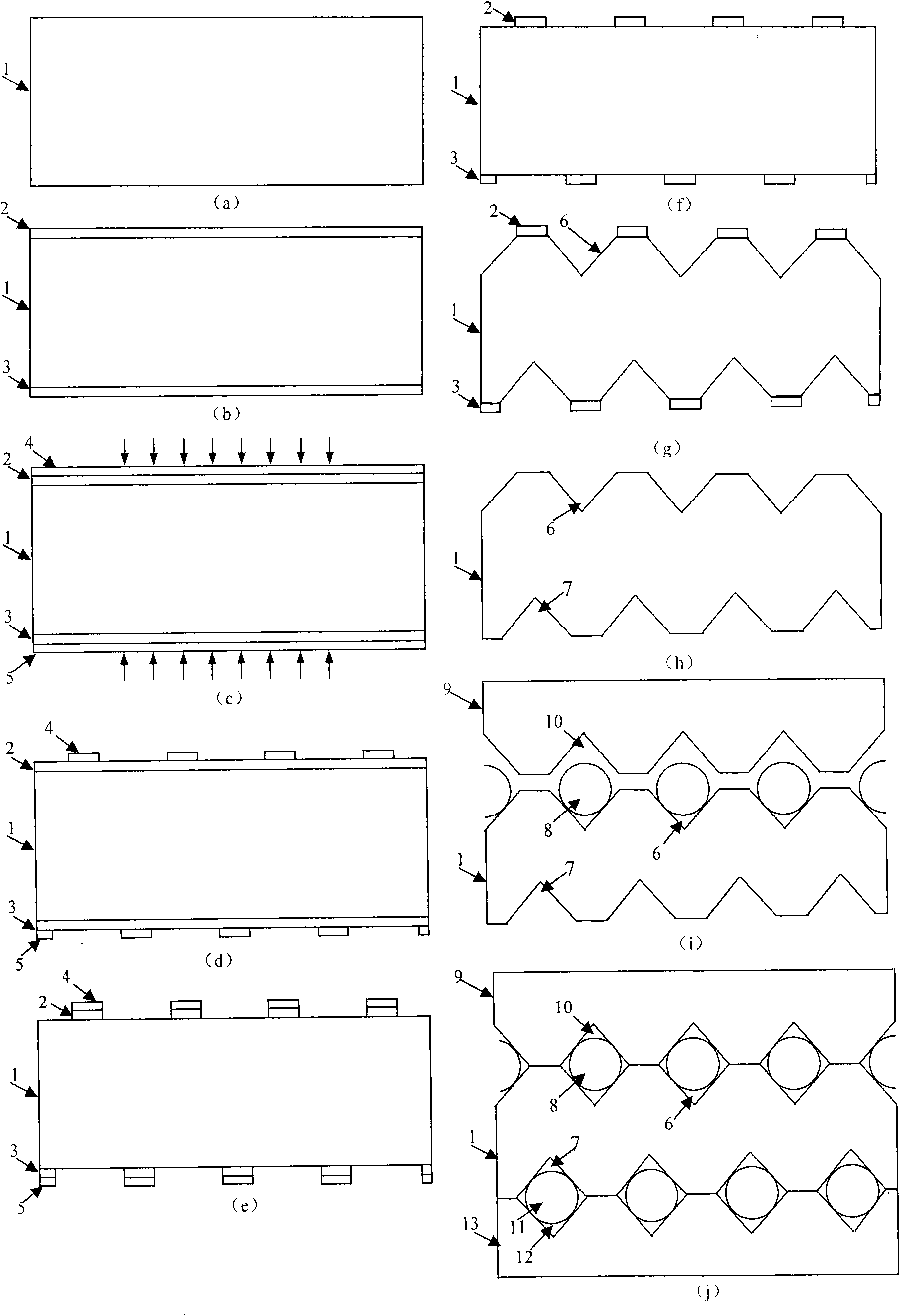
[0035] In order to make the object, technical solution and advantages of the present invention clearer, the present invention will be described in further detail below in conjunction with specific embodiments and with reference to the accompanying drawings.

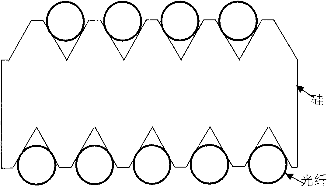
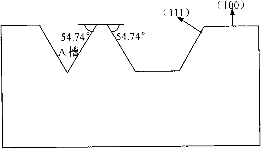
[0036] figure 1 It is a schematic cross-sectional view of the double-layer optical fiber array proposed by the present invention. Such as figure 1 As shown, the two rows of V-shaped grooves of the double-layer optical fiber array are respectively located on the upper and lower surfaces of the same silicon chip, and the bottom angle of the V-shaped grooves is 70.52°. The positions of the column V-grooves can be in one-to-one correspondence, or can be staggered by a certain distance, such as 62.5 microns. One optical fiber is placed in each V-shaped groove, and the end polishing angle of the two-dimensional double-layer optical fiber array is 0° or 8°. Secure with UV-curable glue.

[0037] The invention also proposes a ...


PUM

PropertyMeasurementUnit
Thicknessaaaaaaaaaa
Widthaaaaaaaaaa

Abstract

The invention relates to a two-dimensional double-layer fiber array and a method for manufacturing the same. The two-dimensional double-layer fiber array is manufactured on the same silicon chip; the fiber array is divided into an upper layer and a lower layer; a plurality of fibers can be placed in each layer; and each layer is fixed and protected by a cover plate. The double-layer fiber array applies double-side photoetching and anisotropic etching technology of a silicon process to manufacture a layer of the fiber array on the upper bottom surface and the lower bottom surface of the silicon chip respectively; each layer of the fiber array consists of at least one V-shaped groove; and the fibers are placed and fixed inside the V-shaped groove. The proposal, effectively improves the density of the fiber array and saves the space.

Description

technical field [0001] The invention relates to the field of semiconductor devices, in particular to a two-dimensional double-layer optical fiber array and a manufacturing method thereof. Background technique [0002] Integrated optical devices have been widely used in many fields. In the manufacturing process of devices, the coupling between pigtails and chips is one of the key technologies. Because the optical fiber is very thin, when the optical fiber is coupled with the chip, there must be a clamp that can clamp and position. When coupling, the clamp and the optical fiber are bonded together with the chip as a whole, which can increase the bonding area and improve the reliability of the device. reliability. The size of the fixture is very small, and the accuracy requirements are also on the order of microns. Si single crystal material is widely used because of its special microscopic mechanism, especially the convenience of microfabrication with semiconductor technolog...

Claims


Application Information

Patent Timeline
IPC IPC(8): G02B6/12G02B6/13G03F7/00
Inventor 耿敏明张磊杨林田贺斌王桐刘育梁
Owner INST OF SEMICONDUCTORS - CHINESE ACAD OF SCI
Why Eureka
Try Eureka