Printing wiring cardinal plate and method for producing the same
A technology of printed wiring and manufacturing method, applied in the direction of printed circuit manufacturing, printed circuit, printed circuit components, etc., can solve the problems of low chromium content, short circuit, insufficient insulation reliability, etc., to achieve high utilization value, ensure Effects of insulation reliability and excellent corrosion resistance
- Summary
- Abstract
- Description
- Claims
- Application Information
AI Technical Summary
Problems solved by technology
Method used
Image
Examples
Embodiment 1
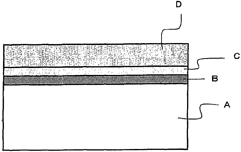
[0135] A polyimide film with a thickness of 38 μm (“Kapton 150EN” manufactured by Toray Dupont Co., Ltd.) was placed on the sputtering device, and the vacuum was exhausted to 1×10 -1 After Pa, heat the polyimide film with an infrared heater, remove the moisture in the film, and then vacuum exhaust to 1×10 -4 Pa. Next, Ar gas was introduced to maintain the pressure in the apparatus at 0.3 Pa, and a Ni-7 mass % Cr layer with a film thickness of 10 nm and a Ni-18 The mass % Cr-10 mass % Mo layer and the copper film layer with a film thickness of 0.1 μm were taken out from the sputtering apparatus. Next, a copper layer with a film thickness of 8 μm was formed on the copper film layer by electroplating to obtain an insulating film metal film laminated body 1 .
[0136] A peel strength measurement sample and an insulation reliability measurement sample were manufactured from the obtained resin film metal film laminated substrate 1, and each test was provided.
[0137] Since the i...
Embodiment 2
[0141] In addition to using Ni-7 mass % Cr with a film thickness of 3 nm for the metal layer B, and Ni-20 mass % Cr with a film thickness of 10 nm for the metal layer C, the resin film metal film laminated substrate 2 obtained by forming a metal film, and the implementation Samples were produced in the same manner as in Example 1, and various tests were performed. Table 1 shows the results.
Embodiment 3
[0143] Samples were produced in the same manner as in Example 1, except that the metal layer B was made of Ni with a film thickness of 5 nm, and the metal layer C was formed with a metal film of Ni-20 mass % Cr with a film thickness of 20 nm. , each test was carried out, and the results are shown in Table 1.
PUM
| Property | Measurement | Unit |
|---|---|---|
| thickness | aaaaa | aaaaa |
| thickness | aaaaa | aaaaa |
| thickness | aaaaa | aaaaa |
Abstract
Description
Claims
Application Information


