Semiconductor power conversion device
A power conversion device, semiconductor technology, applied in the direction of output power conversion device, pulse technology, electronic switch, etc.
- Summary
- Abstract
- Description
- Claims
- Application Information
AI Technical Summary
Problems solved by technology
Method used
Image
Examples
Embodiment approach 1
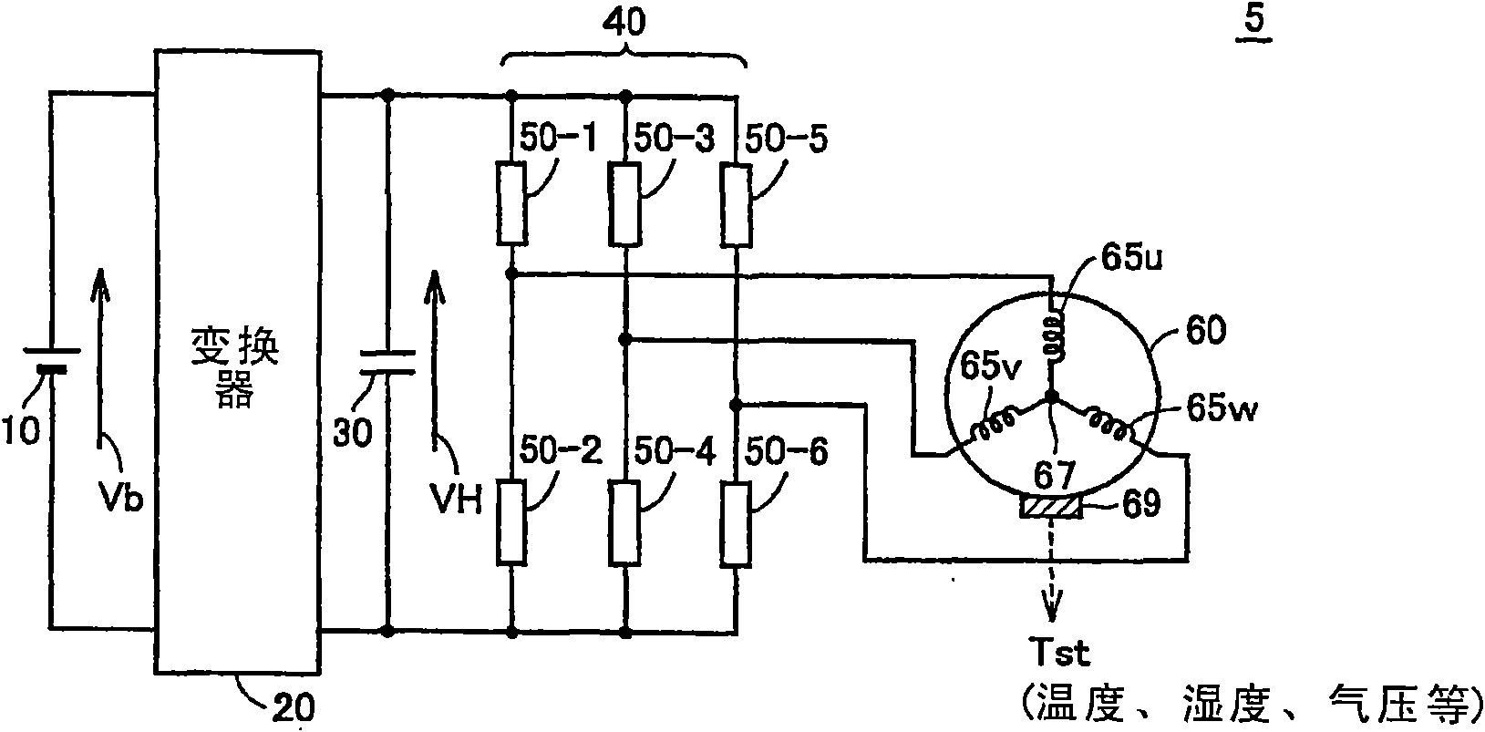
[0060] figure 1 It is a circuit diagram showing a configuration example of the semiconductor power conversion device according to the embodiment of the present invention.
[0061] refer to figure 1 The power conversion system 5 includes: a DC power supply 10, a converter 20, a smoothing capacitor 30, an inverter 40 shown as a representative example of a semiconductor power conversion device according to an embodiment of the present invention, and the inverter 40 is driven and controlled. The electric motor 60.
[0062] The DC power supply 10 outputs a DC voltage Vb. Converter 20 has a DC voltage conversion function, and performs voltage conversion on output voltage Vb from DC power supply 10 to output DC voltage VH. The output voltage of converter 20 is smoothed by smoothing capacitor 30 .
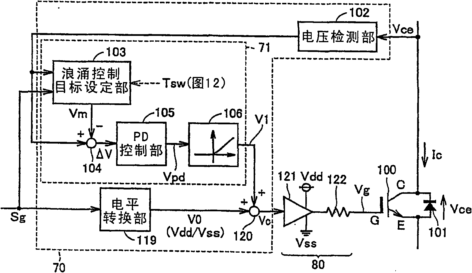
[0063] Inverter 40 has six arms 50-1 to 50-6 constituting upper and lower arms of three phases, respectively. As will be described later, each of the bridge arms 50 (generally referred ...
Embodiment approach 2
[0103] In Embodiment 2, an active gate control that can directly limit the voltage change rate, which is the time differential value of the inter-terminal voltage Vce of the semiconductor switching element 100, by setting a control target for the voltage change rate will be described. .
[0104] Figure 6 It is a block diagram for explaining the switching control configuration of each arm of the semiconductor power conversion device according to Embodiment 2 of the present invention.
[0105] refer to Figure 6 , in the switch control structure according to Embodiment 2, the drive control unit 70 includes a voltage differential unit 107, a voltage increase rate control target setting unit 110, an active gate control unit 72, a voltage drop rate control target setting unit 115, and active gate control section 73 to replace the figure 1 The active gate control part 71 in. Like the active gate control unit 71 , the constituent elements of the voltage differentiating unit 107 ...
Embodiment approach 3
[0138] Figure 10 It is a block diagram for explaining the switching control configuration of each arm of the semiconductor power conversion device according to the third embodiment.
[0139] refer to Figure 10 , in the switch control structure involved in Embodiment 3, with Figure 6 Compared with the switch control structure according to the illustrated second embodiment, the drive control unit 70 is further provided with changeover switches 108 and 109 . The selector switches 108 and 109 may be configured by either hardware or software.
[0140] The selector switch 108 switches the input to the voltage calculation unit 111 between the voltage change rate dVce / dt output from the voltage differential unit 107 and the ground level (GND). When the voltage change rate dVce / dt is input to the voltage calculation unit 111 by switching the switch 108 ( Figure 10 I side), the active gate control unit 72 generates the voltage correction amount V2 by the same feedback control as...
PUM
 Abstract
Description
Claims
Application Information
 - R&D
- Intellectual Property
- Life Sciences
- Materials
- Tech Scout
- Unparalleled Data Quality
- Higher Quality Content
- 60% Fewer Hallucinations
Browse by: Latest US Patents, China's latest patents, Technical Efficacy Thesaurus, Application Domain, Technology Topic, Popular Technical Reports.
© 2025 PatSnap. All rights reserved.Legal|Privacy policy|Modern Slavery Act Transparency Statement|Sitemap|About US| Contact US: help@patsnap.com


