Movable optical element adjusting and positioning device

A technology for adjusting positioning and optical components, which is applied to optical components, optics, photolithography process exposure devices, etc., can solve the problems of high cost of adjusting positioning devices, small adjustment and positioning range, and inaccurate positioning, and achieves compact structure and stable operation. , good repeatability

Active Publication Date: 2009-12-23
SHANGHAI MICRO ELECTRONICS EQUIP (GRP) CO LTD
View PDF2 Cites 32 Cited by
  • Summary
  • Abstract
  • Description
  • Claims
  • Application Information

AI Technical Summary

Problems solved by technology

[0007] The technical problem to be solved by the present invention is to realize the adjustment and positioning of the movable optical element, and solve the problems of high cost, complex structure, small adjustment and positioning range, and inaccurate positioning of the adjustment and positioning device.

Method used


Image

  • Movable optical element adjusting and positioning device
  • Movable optical element adjusting and positioning device
  • Movable optical element adjusting and positioning device

Examples


Embodiment Construction

[0021] In order to make the object, technical solution and advantages of the present invention clearer, the present invention will be further described in detail below in conjunction with the accompanying drawings.

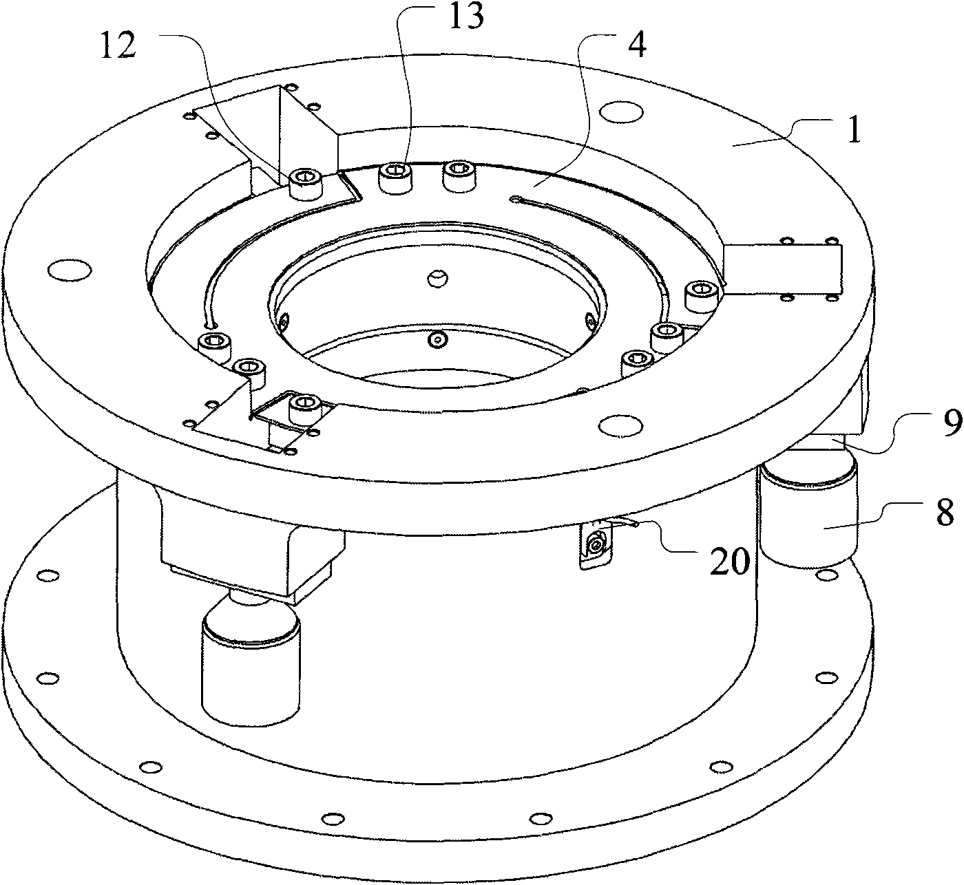
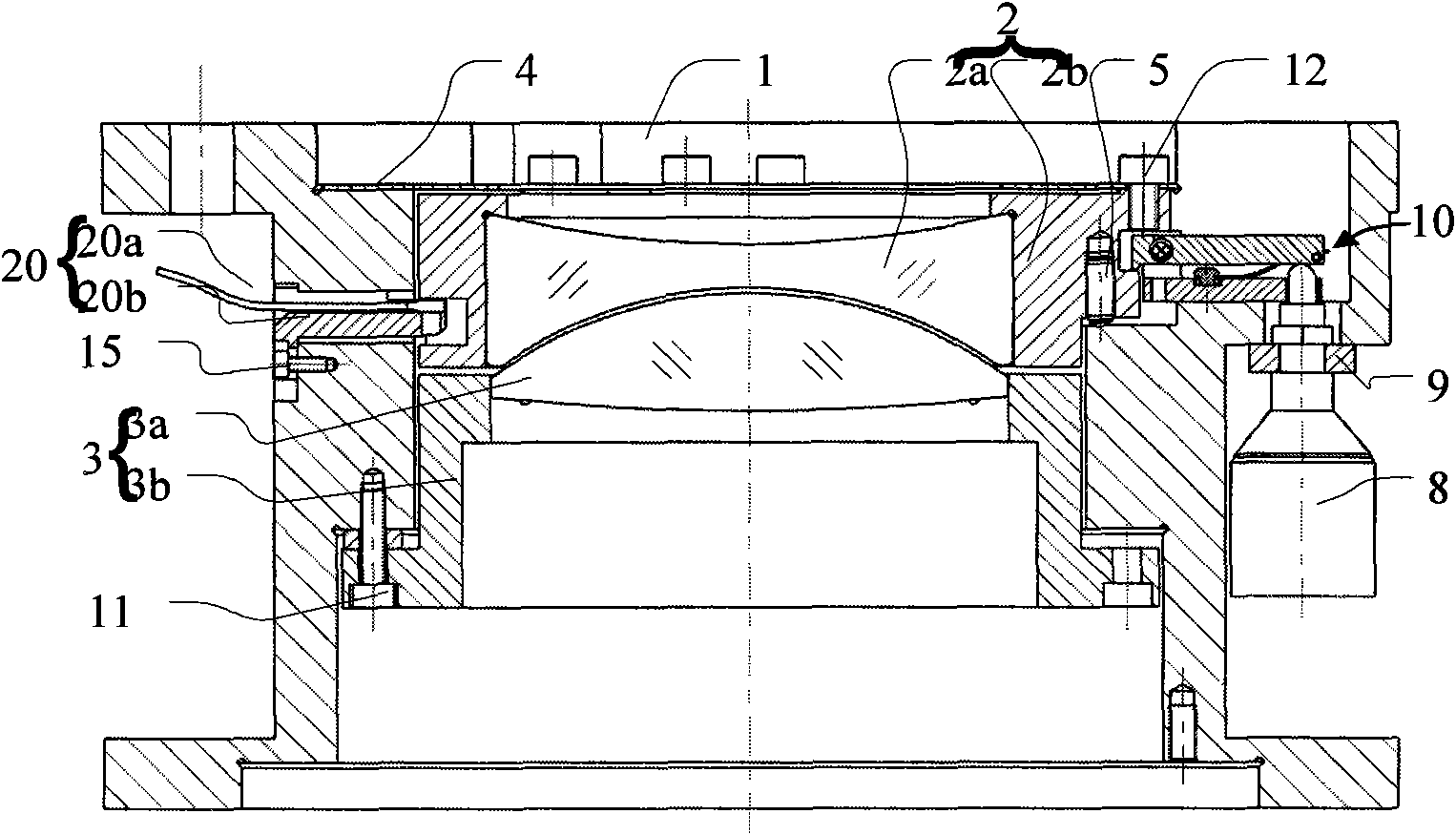
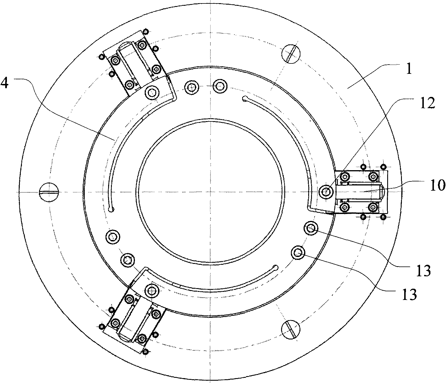
[0022] figure 1 The basic structure diagram of the adjustable positioning device for the movable optical element, figure 2 is a cross-sectional view of the basic structure, image 3 It is the bottom view of the basic structure, Figure 4 A schematic diagram of the motor drive mechanism.

[0023] combined reference Figure 1~4 , this embodiment provides an axial adjustment and positioning device for optical elements in exposure equipment, the device is to adjust the position of the movable mirror group lens 2a relative to the fixed mirror group lens 3a, including axial adjustment and horizontal tilt adjustment.

[0024] The axial adjustment and positioning device of the movable optical element mainly includes: the main lens barrel 1, the movable mirror group 2...


PUM


Abstract

A movable optical element adjusting and positioning device relates to a photoetching apparatus. A movable lens set in the device is fixed on a main lens cone by a laminated spring plate and can move along an optical axis or carry out horizontal inclination adjustment under the action of a driving motor. The driving of the driving motor adopts a long handle of a level mechanism in a driving mechanism of a gapless flexible bearing, and a short handle thereof drives the movable lens set to move along the optical axis. The adjusting and positioning device achieves an axial movement accuracy which can be lower than 0.5 microns and a horizontal adjustment accuracy which can reach 0.5mrad. The adjusting and positioning device has compact structure, stable operation, no friction or lubrication, low hysteresis and good repeatability, and the movement stroke of the movable lens set can reach 0.2 mm and the linearity is good.

Description

technical field [0001] The invention relates to a lithography equipment, in particular to a device for adjusting and positioning a movable optical element in the exposure equipment of a lithography machine. . Background technique [0002] In semiconductor device preparation and mask manufacturing processes, photolithography steps using exposure equipment are essential. In this photolithography step, the substrate material coated with photosensitive materials such as photoresist is processed, that is, the pattern on the reticle is illuminated by the illumination optical system, and the pattern is transferred by the projection optical system. onto the semiconductor substrate. [0003] In recent years, with the integration level of semiconductor devices getting higher and higher, the feature size of the devices is getting smaller and smaller, and the precision requirements for pattern transfer are also getting higher and higher. The projection optical system in the exposure ...

Claims


Application Information

Patent Timeline
Patent Type & Authority Applications(China)
IPC IPC(8): G02B7/02G03F7/20
Inventor 谭长永王洪尊
Owner SHANGHAI MICRO ELECTRONICS EQUIP (GRP) CO LTD
Why Eureka
Try Eureka