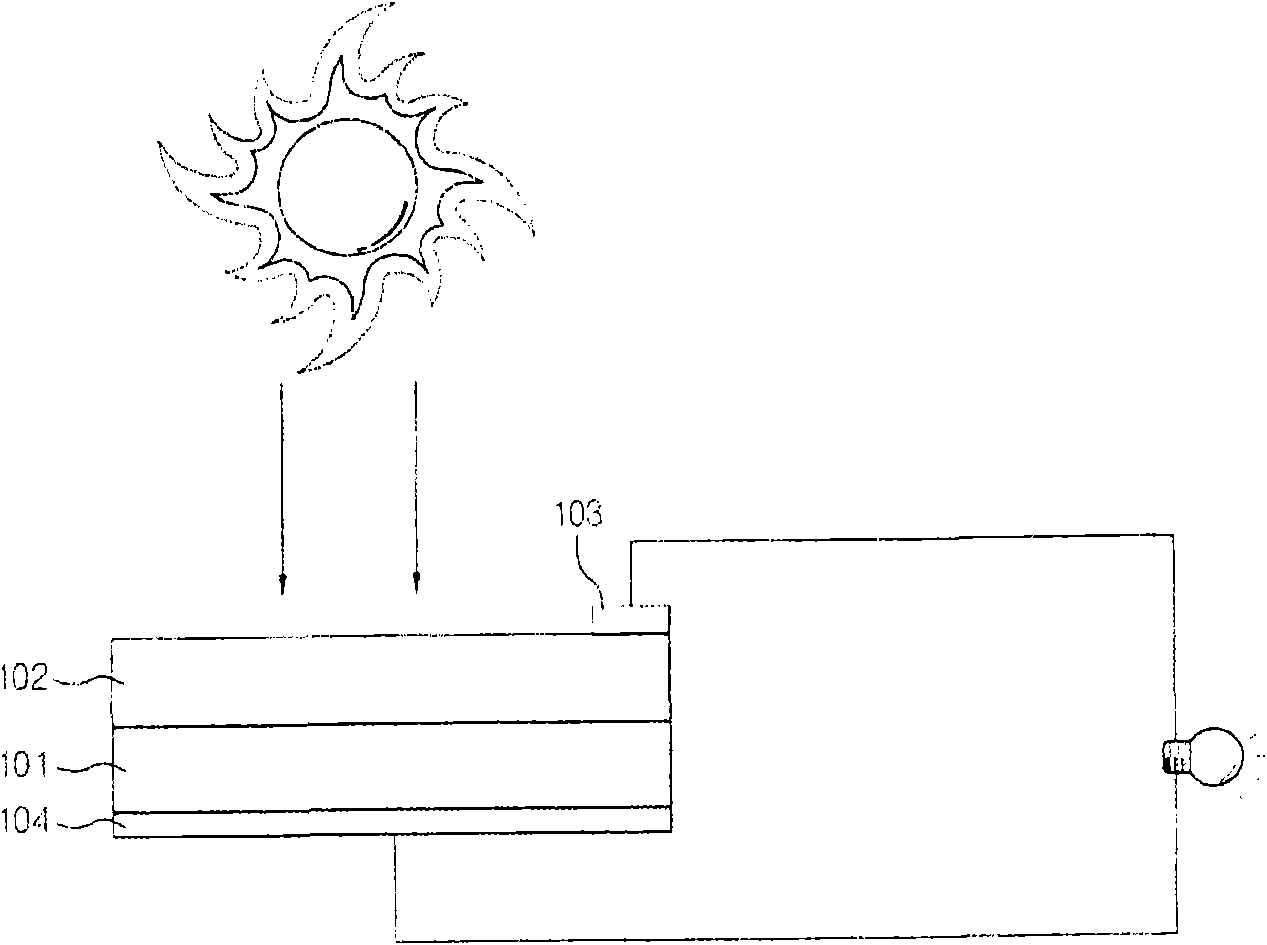
Solar cell

A solar cell, conductive technology, applied in the field of solar cells, can solve problems such as the reduction of sunlight ratio, the reduction of solar cell efficiency, and the limitation of anti-reflection film structure

Inactive Publication Date: 2009-12-23
LG ELECTRONICS INC
View PDF1 Cites 11 Cited by
  • Summary
  • Abstract
  • Description
  • Claims
  • Application Information

AI Technical Summary

Problems solved by technology

However, when the microelectronic layer has the above-mentioned refractive index distribution, on the contrary, the ratio of sunlight reaching the p-n junction structure that produces the photoelectric effect decreases, and the efficiency of the solar cell decreases.
The reason is that when sunlight is incident on the microelectronic layer, part of the light is guided along the plane through the intermediate layer with a relatively large refractive index, so that the ratio of sunlight reaching the p-n junction decreases.
Moreover, the microelectronic layer of this U.S. patent is limited when used as an anti-reflection film structure for high-efficiency solar cells

Method used


Image

  • Solar cell
  • Solar cell
  • Solar cell

Examples


Embodiment 1

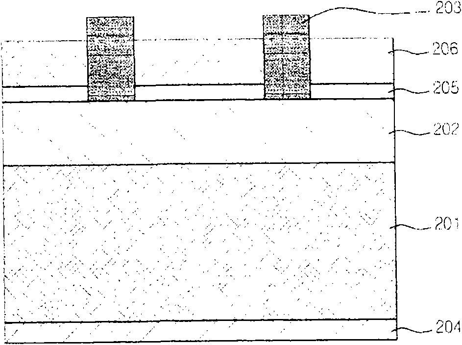
[0035] Made as figure 2 A solar cell with a passivation layer and an anti-reflection film is shown. At this time, as the semiconductor substrate, Cz mono 125×125cm was used 2 A p-type silicon substrate (0.5-2Ω) is used to form an n+ emission layer with 60Ω / sheet. Using Direct High Frequency (13.56MHz) PECVD, a silicon oxynitride passivation layer (refractive index: 1.55, thickness: 30nm) is formed on the above-mentioned emission layer, and a silicon nitride anti-reflection film (refractive index: 30nm) is formed on the above-mentioned passivation layer 1.90, thickness: 64nm). The deposition temperature of the above-mentioned passivation layer and anti-reflection film is 350°C. Then, an electrode pattern was coated on the anti-reflection film by screen printing, and an aluminum electrode was coated on the reverse side of the surface of the semiconductor substrate on which the reflection layer was formed by screen printing, and the anti-reflection coating was carried out at ...

Embodiment 2

[0037] Made as figure 2 A solar cell with a passivation layer and an anti-reflection film is shown. At this time, as the semiconductor substrate, Cz mono 125×125cm was used 2 A p-type silicon substrate (0.5-2Ω) is used to form an n+ emission layer with 60Ω / sheet. Using Direct High Frequency (13.56MHz) PECVD, a silicon oxynitride passivation layer (refractive index: 1.65, thickness: 25nm) is formed on the above-mentioned emission layer, and a silicon nitride anti-reflection film (refractive index: 25nm) is formed on the above-mentioned passivation layer 1.90, thickness: 64nm). The deposition temperature of the above-mentioned passivation layer and anti-reflection film is 350°C. Then, an electrode pattern was coated on the anti-reflection film by screen printing, and an aluminum electrode was coated on the reverse side of the surface of the semiconductor substrate on which the reflection layer was formed by screen printing, and the anti-reflection coating was carried out at ...


PUM


Abstract

A solar cell includes a p-n structure having a first conductive semiconductor substrate, a second conductive semiconductor layer formed on the first conductive semiconductor substrate and having a conduction opposite to the first conductive semiconductor substrate, and a p-n junction formed at an interface between the first conductive semiconductor substrate and the second conductive semiconductor layer; a passivated layer formed on the second conductive semiconductor layer and composed of silicon oxynitride with a refractive index of 1.45 to 1.70; an anti-reflection film formed on the passivated layer and composed of silicon nitride; a front electrode connected to the second conductive semiconductor layer with passing through a part of the passivated layer and the anti-reflection film and exposed outward; and a rear electrode formed at an opposite side to the front electrode with the first conductive semiconductor substrate being interposed therebetween to be connected to the first conductive semiconductor substrate.

Description

technical field [0001] The invention relates to a solar cell, in particular to a solar cell with excellent photoelectric conversion efficiency. The solar cell has an improved anti-reflection film, thereby reducing the reflectivity to sunlight and increasing the FF value. Background technique [0002] In recent years, with the shortage of existing resources such as oil and coal, attention to alternative energy sources to replace them has gradually increased. Among them, solar cells have attracted much attention because they are rich in energy and do not cause environmental pollution. Solar cells are divided into solar thermal cells and solar photovoltaic cells. The so-called solar thermal cells use solar heat to generate the steam required for rotating turbines. The so-called solar cells use the properties of semiconductors to convert sunlight (photons) into electrical energy. , Usually solar cells refer to solar photovoltaic cells (hereinafter referred to as solar cells). ...

Claims


Application Information

Patent Timeline
Patent Type & Authority Applications(China)
IPC IPC(8): H01L31/042
CPCH01L31/022425H01L31/02168Y02E10/52H01L31/068H01L31/02167G02B1/113H01L31/1868Y02E10/547Y02P70/50H01L31/04H01L31/06H01L31/18
Inventor 朴铉定金圣辰金振镐
Owner LG ELECTRONICS INC
Why Eureka
Try Eureka