Trench gate metal oxide semiconductor field effect transistor and manufacturing method thereof

An oxide semiconductor and field effect transistor technology, which is applied in the structural field of metal oxide semiconductor field effect transistors, can solve problems such as inconvenience, transistor failure, coverage, etc., and achieves the effects of technological progress, manufacturing method improvement, and manufacturing method enhancement.

Inactive Publication Date: 2010-02-24
NIKO SEMICON
View PDF0 Cites 6 Cited by
  • Summary
  • Abstract
  • Description
  • Claims
  • Application Information

AI Technical Summary

Problems solved by technology

In the traditional manufacturing process of metal oxide semiconductor field effect transistors, the concentration of the P-type dopant is relatively high at the two sides 122b adjacent to the gate trench 130. Therefore, the P-type well region 122 is formed when the dopant is introduced. During the process, the bottom of the gate trench 130 is easily covered by the P-type well region 122, resulting in transistor failure
[0011] Therefore, how to improve the depth distribution of the well region of the metal oxide semiconductor field effect transistor and avoid the failure of the transistor caused by the well region covering the bottom of the gate trench is an urgent goal pursued by ...

Method used


Image

  • Trench gate metal oxide semiconductor field effect transistor and manufacturing method thereof
  • Trench gate metal oxide semiconductor field effect transistor and manufacturing method thereof
  • Trench gate metal oxide semiconductor field effect transistor and manufacturing method thereof

Examples


Embodiment Construction

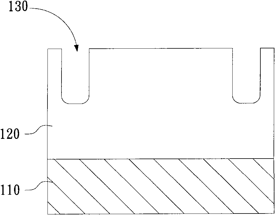
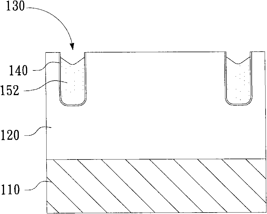
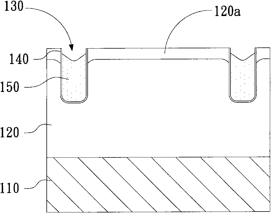
[0069] In order to further illustrate the technical means and effects that the present invention adopts to achieve the intended invention purpose, the trench-gate metal-oxide-semiconductor field-effect transistor and its manufacturing method according to the present invention are described below in conjunction with the accompanying drawings and preferred embodiments. The specific implementation, structure, manufacturing method, steps, features and effects thereof are described in detail below.

[0070] The aforementioned and other technical contents, features and effects of the present invention will be clearly presented in the following detailed description of preferred embodiments with reference to the drawings. Through the description of the specific implementation mode, when the technical means and functions adopted by the present invention to achieve the predetermined purpose can be obtained a deeper and more specific understanding, but the accompanying drawings are only f...


PUM


Abstract

The invention relates to a trench gate metal oxide semiconductor field effect transistor and a manufacturing method thereof. The method comprises the following steps: manufacturing a first conductiveepitaxial layer on a silicon substrate; manufacturing a plurality of trenches on the epitaxial layer; performing overall ion implantation of a first conductive doping material on the epitaxial layer;manufacturing a polysilicon pattern layer covering the trenches and the epitaxial layer in a preset range around the trenches; implanting a second conductive doping material on the epitaxial layer through the polysilicon pattern layer; importing a doping material to form a well area having the second conductive doping material; implanting the first conductive doping material in the well area through the polysilicon pattern layer to form a plurality of first doped areas; implanting the doping material of the first doped areas to form source electrode doped areas close to the trenches; and removing the polysilicon pattern layer above the epitaxial layer to form a polysilicon gate. The method can improve the depth distribution of the sell area of the trench gate metal oxide semiconductor field effect transistor and avoiding the effectiveness loss caused by the coverage of the gate trenches by the well area.

Description

technical field [0001] The invention relates to a metal oxide semiconductor field effect transistor (MOS) structure and a manufacturing method thereof, in particular to a method for avoiding well coverage by improving the depth distribution of the well area of ​​the trench gate metal oxide semiconductor field effect transistor The structure and fabrication method of a trench-gate metal-oxide-semiconductor field-effect transistor (Trench MOS) in which the transistor fails due to the bottom of the gate trench. Background technique [0002] In order to meet the needs of energy saving and system power loss reduction, higher energy conversion efficiency is required. These design specification requirements that keep pace with the times will become increasingly severe challenges for power converter designers. To meet this demand, new power components play an increasingly important role in high-efficiency converters. Among them, power metal oxide semiconductor field effect transist...

Claims


Application Information

Patent Timeline
IPC IPC(8): H01L21/336H01L29/78H01L29/06
Inventor 涂高维董正晖蔡筱薇
Owner NIKO SEMICON
Why Eureka
Try Eureka