Multilayer interconnection structure of wafer level package, manufacturing method and application

A technology of wafer-level packaging and multilayer interconnection, which is applied in semiconductor/solid-state device manufacturing, electrical components, electric solid-state devices, etc., can solve problems such as large parasitic effects and large losses, and reduce parasitic effects and losses, reduce Loss, the effect of increasing packing density and production efficiency

Inactive Publication Date: 2010-02-24
SHANGHAI INST OF MICROSYSTEM & INFORMATION TECH CHINESE ACAD OF SCI
View PDF1 Cites 21 Cited by
  • Summary
  • Abstract
  • Description
  • Claims
  • Application Information

AI Technical Summary

Problems solved by technology

Active circuit chips such as MMIC usually realize the electrical interconnection between the chip and the substrate circuit through a wire bonding connection. The disadvantage of the wire bonding connection is that i

Method used


Image

  • Multilayer interconnection structure of wafer level package, manufacturing method and application
  • Multilayer interconnection structure of wafer level package, manufacturing method and application
  • Multilayer interconnection structure of wafer level package, manufacturing method and application

Examples


Example Embodiment

[0032] The embodiments of the present invention will be further described in detail below with reference to the accompanying drawings to fully embody the advantages and positive effects of the present invention. The scope of the present invention is not limited to the following embodiments.

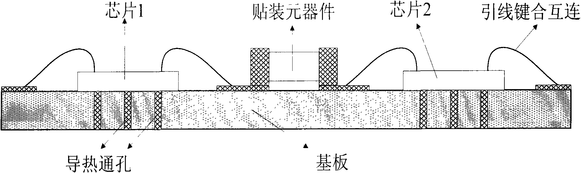
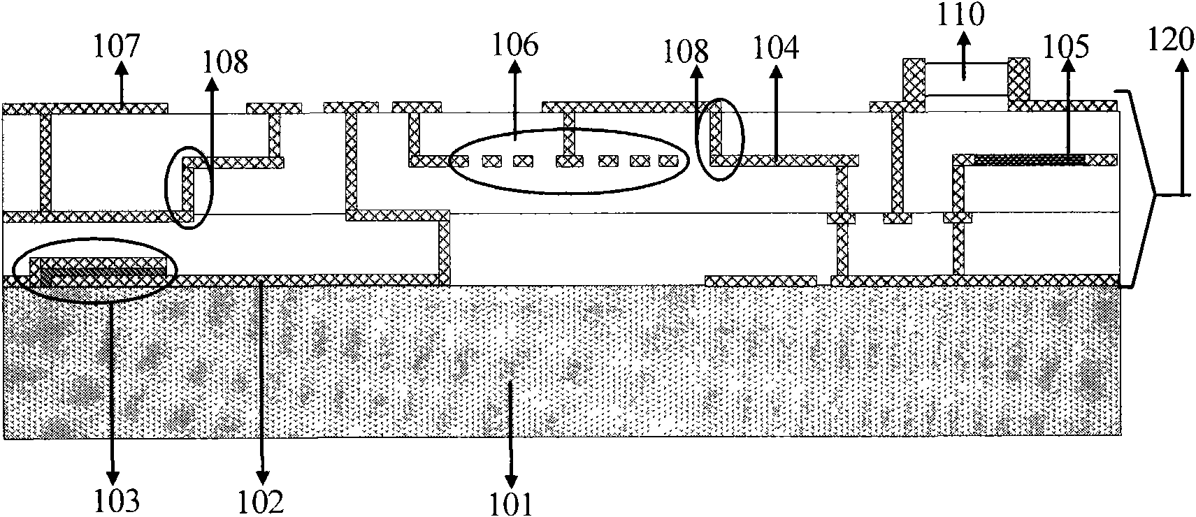
[0033] Such as figure 2 Shown is a microwave multi-chip module wafer-level package structure according to an embodiment of the present invention. The multi-layer interconnection structure 120 based on the silicon substrate 101 is embedded with a transmission line 104 for interconnection, a ground layer 102, and various passive components, such as a capacitor 103, a resistor 105, an inductor 106, and a miniature antenna 107. The metal interconnections (such as the transmission lines 104 and the vertical interconnect vias 108) and the passive components in the multilayer interconnection structure are realized by a low-cost electroplating process. The thickness of the metal is generally 1 to ...


PUM

PropertyMeasurementUnit
Thicknessaaaaaaaaaa
Thicknessaaaaaaaaaa

Abstract

The invention provides a multilayer interconnection structure of wafer level package, a manufacturing method and application thereof. The multilayer interconnection structure is used for microwave multi chip modules. The invention is characterized by using benzocyclobutene (BCB) as a dielectric layer, realizing the multilayer connection structure of a metal/organic polymer by combining wafer levelprocessing technics such as photoetching, electroplating, mechanical polishing and the like and embedding integrated varied passive devices and transmission lines for interconnection. The whole process is matched with IC process, is completed on the basis of wafer level and has higher integration of packaging and lower high-frequency transmission loss. The structure can effectively integrate varied function device units, reduce the interconnection loss among the devices and improve the properties of the whole module while improving the density and integration of packaging and reducing the cost of packaging.

Description

technical field [0001] The invention relates to a multi-layer interconnection structure, preparation method and application for microwave multi-chip module (Microwave Multi Chip Module, abbreviated as MMCM) wafer-level packaging. In particular, it relates to multilayer three-dimensional packaging structures including micromachining techniques such as mechanical polishing. Background technique [0002] Multi-chip module (Multi Chip Module, abbreviated as MCM), refers to the integration of multiple bare or / and packaged integrated circuit chips and single or multiple passive components, such as resistors, capacitors, inductors, etc., into a package substrate A technique on which a system or functional module is formed, figure 1 Shown is a schematic dissection diagram of a traditional MCM. Chips and components are mounted on a substrate, and the interconnection between the chip and the substrate or the chip and other devices is realized by wire bonding. Microwave Multi Chip Mo...

Claims


Application Information

Patent Timeline
IPC IPC(8): H01L25/00H01L27/00H01L23/522H01L21/50H01L21/60
CPCH01L2224/48091H01L2224/48227H01L2924/19105H01L2924/3025H01L2924/30107
Inventor 丁晓云耿菲罗乐
Owner SHANGHAI INST OF MICROSYSTEM & INFORMATION TECH CHINESE ACAD OF SCI
Why Eureka
Try Eureka