Preparation method of integral GaN-based film

An integrity, epitaxial thin film technology, applied in chemical instruments and methods, crystal growth, electrical components, etc., can solve problems such as edge damage of unit GaN-based epitaxial thin films, and achieve the effect of reducing cracks, ensuring integrity, and improving yield

Active Publication Date: 2010-03-03
XIAMEN SANAN OPTOELECTRONICS TECH CO LTD
View PDF0 Cites 16 Cited by
  • Summary
  • Abstract
  • Description
  • Claims
  • Application Information

AI Technical Summary

Problems solved by technology

[0004] In order to solve the problem of edge damage of the unit GaN-based epitaxial film existing in the laser lift-off sapphire substrate, the present invention innovatively proposes a method for preparing a complete GaN-based epitaxial film, including steps:

Method used


Image

  • Preparation method of integral GaN-based film
  • Preparation method of integral GaN-based film
  • Preparation method of integral GaN-based film

Examples


Embodiment Construction

[0022] The present invention will be further described below in conjunction with the accompanying drawings and embodiments.

[0023] A method for preparing a complete GaN-based epitaxial film, the preparation steps are as follows:

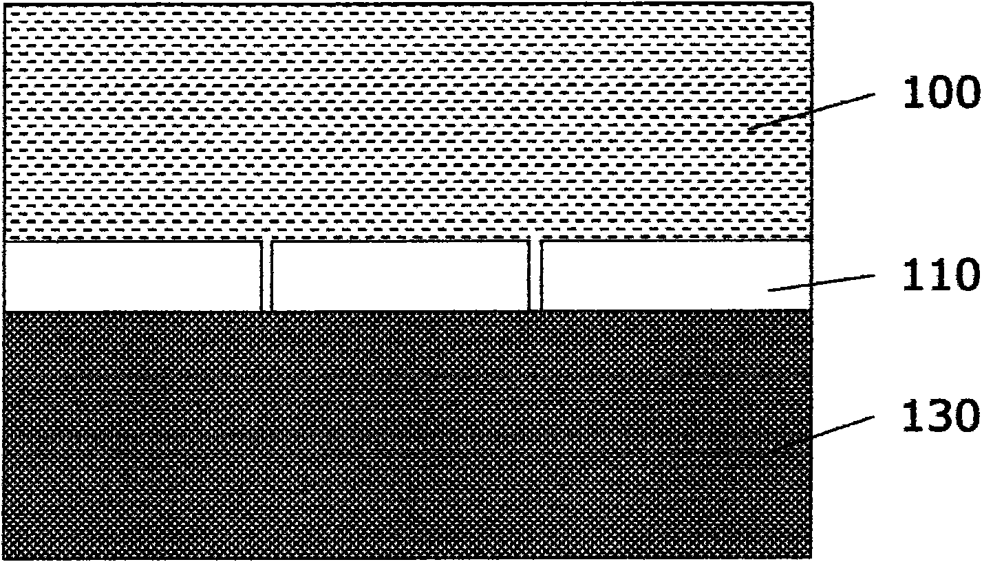
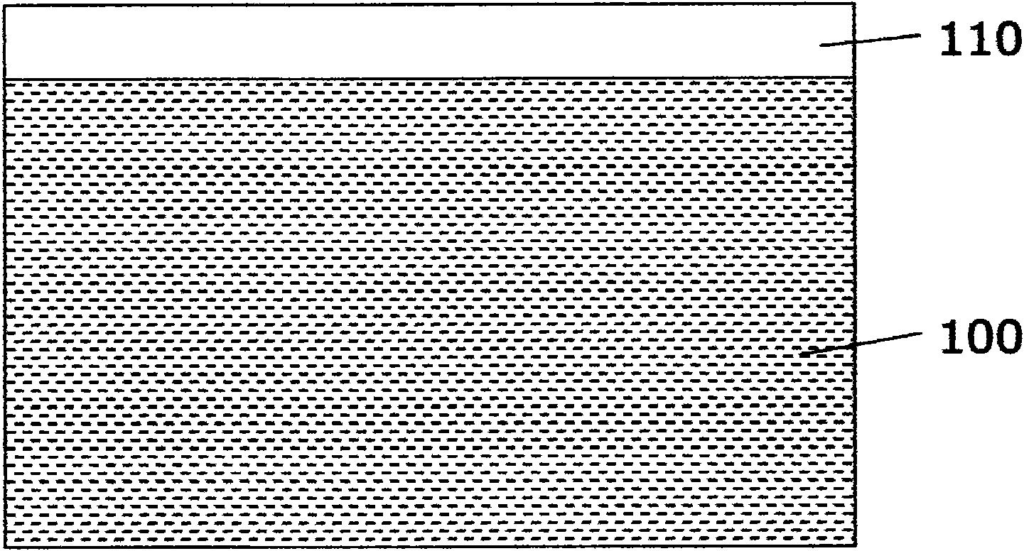
[0024] Such as Figure 2a As shown, an N-type GaN-based semiconductor layer, an active layer, and a P-type GaN-based semiconductor layer are sequentially epitaxially grown on a sapphire substrate 100 by metal-organic chemical vapor deposition (MOCVD) to form a GaN-based LED epitaxial layer 110;

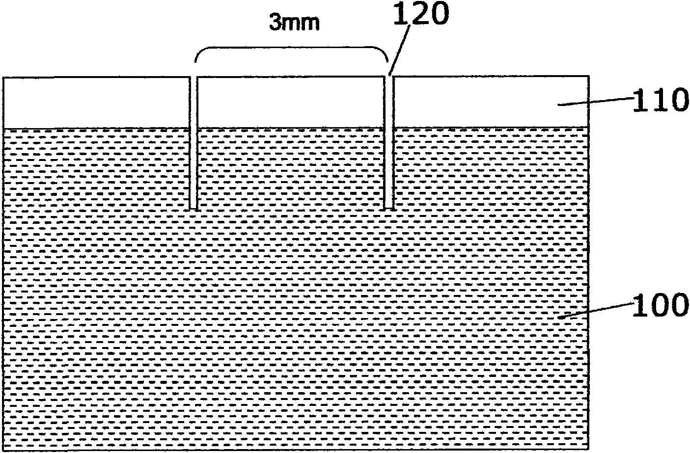
[0025] Such as Figure 2b As shown, a laser scriber (wavelength 355nm) is used to scribe from the GaN-based epitaxial layer 110 and extend to the sapphire substrate 100. The scribing is carried out in an orthogonal (X-Y axis) manner with a period of 3mm×3mm, and the set The laser stripping spot size is similar, and the depth of the laser scribing is 30 microns, that is, the preset channel 120 is formed, and its plan view is as follows image 3 shown;

...


PUM

PropertyMeasurementUnit
thicknessaaaaaaaaaa
thicknessaaaaaaaaaa

Abstract

The invention discloses a preparation method of an integral GaN-based film. a channel is preset in the unit spot edge area, on one hand, the break of a GaN extension wafer or a supporting substrate caused during transferring the substrate by eutectic bonding can be greatly reduced; on the other hand, after the substrate is transferred, the preset channel is naturally exposed by thinning a sapphiresubstrate, a gas release channel for laser stripping process is provided, and meanwhile, absolute separation of the sapphire substrate in an adjacent spot area and the extension film thereof is realized; and the stripping units are independent and are not influenced by the stress, so the damage problem of the edge of a unit GaN-based film can be solved, that is to say, the integrity of the GaN-based film subjected to laser stripping of the sapphire substrate can be ensured and the finished product rate of a GaN-based film device can be improved.

Description

technical field [0001] The invention relates to a method for manufacturing a GaN-based thin film, and more specifically relates to a preparation method for a GaN-based thin film suitable for removing a sapphire substrate by a laser lift-off technique. Background technique [0002] At present, most gallium nitride (GaN)-based epitaxial materials are mainly grown on sapphire substrates, but due to the poor conductivity of sapphire, ordinary GaN-based light-emitting devices adopt a lateral structure, that is, the two electrodes are on the same side of the device, The current flows in the N-GaN layer for different distances laterally, and there is current blockage, which generates heat; in addition, the poor thermal conductivity of the sapphire substrate greatly limits the luminous power and efficiency of GaN-based devices. In recent years, in order to improve the luminous power and efficiency of GaN chips, laser lift-off (Laser Lift-off, LLO) sapphire technology has been develo...

Claims


Application Information

Patent Timeline
Patent Type & Authority Applications(China)
IPC IPC(8): C30B29/38H01L33/00H01L27/15
Inventor 林雪娇潘群峰吴志强叶孟欣黄慧君陈文欣洪灵愿
Owner XIAMEN SANAN OPTOELECTRONICS TECH CO LTD
Why Eureka
Try Eureka