Method of double-element delta doped growth P-type GaN base material

A technology of base materials and elements, applied in the field of preparation of GaN materials, can solve the problems that are not enough, can not meet the requirements of devices well, difficult to obtain high-quality, high hole concentration P-type GaN-based materials, etc., and achieve self-compensation inhibition. effect of effect

Inactive Publication Date: 2011-07-06
SUN YAT SEN UNIV
View PDF0 Cites 0 Cited by
  • Summary
  • Abstract
  • Description
  • Claims
  • Application Information

AI Technical Summary

Problems solved by technology

At present, the P-type impurity commonly used in GaN-based materials is Mg. Since Mg itself has high ionization energy and the self-compensation effect of Mg impurities is relatively obvious, the hole concentration of Mg-GaN-based materials is usually only 10 17 ~10 18 cm -3 , the mobility is less than 10cm 2 / V s, the doping efficiency is only 0.1% to 1%, which cannot meet the device requirements well, that is, when Mg is used alone as a P-type dopant, it is difficult to obtain high-quality, high-hole-concentration P-type GaN-based materials

Method used


Image

  • Method of double-element delta doped growth P-type GaN base material
  • Method of double-element delta doped growth P-type GaN base material
  • Method of double-element delta doped growth P-type GaN base material

Examples


Embodiment 1

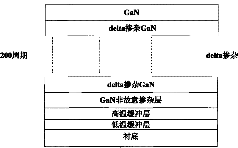
[0024] The present invention adopts metal-organic chemical vapor deposition (MOCVD) method to grow the substrate, low-temperature buffer layer, high-temperature buffer layer and GaN-based material. Surface sapphire substrate, the surface roughness is less than 0.1nm.

[0025] Such as figure 1 and figure 2 shown, using NH 3 , TMGa as N source and Ga source respectively, using H 2 As a carrier gas, the sapphire substrate is first heated to 550°C in the MOCVD reaction chamber, and a low-temperature buffer layer of 0.1um is grown on the sapphire substrate, and the material is GaN. Next, the temperature of the sapphire substrate is heated to 1050° C., and a high-temperature buffer layer of 1 μm is grown on the low-temperature buffer layer, and the material is GaN.

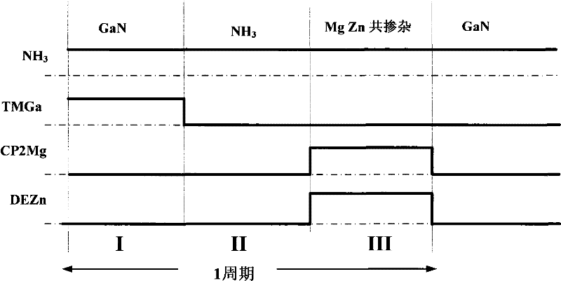
[0026] Secondly, keep the temperature of the sapphire substrate at 1050°C, and grow P-type GaN material for 200 cycles on the upper surface of the high-temperature buffer layer using the double-element delta doping...


PUM


Abstract

The invention discloses a method of double-element delta doped growth P-type GaN base material, comprising the following steps: 1) respectively growing a low-temperature buffer layer and a high-temperature buffer layer on the substrate placed in a reaction cavity; 2) adopting a double-element delta doped method to grow p-type GaN base layer material on the high-temperature buffer layer, wherein, doped elements are Mg, Zn or Mg, O or Mg and Si; 3) adopting a thermal annealing method to activate impurity elements. The method of double-element delta doped growth P-type GaN base material, which is provided by the invention, can obviously inhibit the self-compensating effect of Mg impurities and can simultaneously obtain P-type GaN base material with high quality and high hole concentration.

Description

technical field [0001] The invention relates to the technical field of preparation of GaN materials, in particular to a method for growing P-type GaN-based materials by double-element delta doping. Background technique [0002] GaN is the third generation of new semiconductor materials after the first generation of silicon, germanium and the second generation of gallium arsenide, indium phosphide and other materials. GaN-based materials have wide bandgap, high luminous efficiency, high electron drift saturation velocity, high thermal conductivity, high hardness, small dielectric constant, stable chemical properties, radiation resistance, high temperature resistance, high concentration of two-dimensional electron gas at heterojunction interface, etc. It has become the most important semiconductor material for manufacturing high-power, high-frequency electronic devices, short-wavelength optoelectronic devices, high-temperature devices and radiation-resistant devices, and is kn...

Claims


Application Information

Patent Timeline
Patent Type & Authority Patents(China)
IPC IPC(8): H01L21/205H01L21/22
Inventor 江灏陈计林
Owner SUN YAT SEN UNIV
Why Eureka
Try Eureka