
Double-sided bonding long-wavelength vertical cavity surface emitting laser and manufacturing method thereof

A vertical cavity surface emission, laser technology, applied in lasers, laser parts, semiconductor lasers, etc., can solve the problems of difficult to achieve high reflectivity, difficult epitaxial growth, large thermal resistance, etc., to avoid secondary epitaxy process, The effect of reducing the difficulty of growth

Active Publication Date: 2010-03-10
INST OF SEMICONDUCTORS - CHINESE ACAD OF SCI
View PDF0 Cites 28 Cited by
  • Summary
  • Abstract
  • Description
  • Claims
  • Application Information

AI Technical Summary

Problems solved by technology

[0005] Wafer bonding technology is applied to 1.3μm and 1.55μm wavelength VCSEL, and the Bragg reflector composed of high-reflectivity GaAs / AlGaAs material system is bonded with the InP-based active region, which improves the traditional long-wavelength VCSEL distributed Bragg reflector layer The shortcomings of large number, large thermal resistance, difficulty in achieving high reflectivity, and difficulty in epitaxial growth

Method used


Image

  • Double-sided bonding long-wavelength vertical cavity surface emitting laser and manufacturing method thereof
  • Double-sided bonding long-wavelength vertical cavity surface emitting laser and manufacturing method thereof
  • Double-sided bonding long-wavelength vertical cavity surface emitting laser and manufacturing method thereof

Examples


Embodiment Construction

[0043] In order to make the objectives, technical solutions and advantages of the present invention clearer, the present invention will be further described in detail below with reference to specific embodiments and accompanying drawings.

[0044] Please see attached Figure 1 to Figure 13 . The purpose of the present invention is to provide a double-sided bonding long-wavelength vertical cavity surface emitting laser.

[0045] The structure of the laser is as follows:

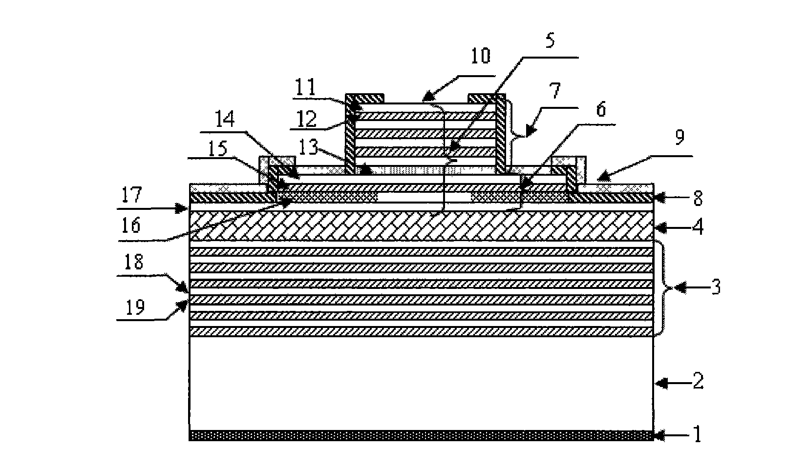
[0046] figure 1 It is a schematic diagram of the double-sided bonding long-wavelength surface emitting laser of the present invention. The laser includes an N-type electrode 1, the N-type electrode is fabricated on the back of an N-type GaAs substrate 2, the N-type GaAs substrate 2, and the N-type GaAs / / Al 0.9 Ga 0.1 As AlGaAs distributed Bragg reflector DBR3, N-type DBR is fabricated on N-type GaAs substrate 2, including 32 periods of N-type GaAs / Al 0.9 Ga 0.1 The As layers 18 and 19 are composed of th...


PUM

PropertyMeasurementUnit
wavelengthaaaaaaaaaa

Abstract

The invention relates to a double-sided bonding long-wavelength vertical cavity surface emitting laser (VCSEL) and a manufacturing method thereof. The laser comprises an N electrode (1), an N-type GaAs substrate (2), an N-type GaAs / AlGaAs material series lower distributed Bragg reflector (DBR) (3), an InP based strained quantum well active area (4), a GaAs / AlGaAs material series upper DBR (5), a SiO2 mask (8), a P electrode (9) and a light-exiting window (10), wherein the upper DBR (5) consists of a P-type DBR (6) and an intrinsic DBR (7). The structure and the method overcome the defects of smaller refractive index difference, poor thermal conductivity and poor electrical conductivity of DBR materials of the conventional VCSEL, not only can realize good current limit, but also can reducethe absorption consumption and the growth difficulty of the materials and omit the step of secondary epitaxial process.

Description

technical field [0001] The invention relates to the technical field of vertical cavity surface emitting lasers, in particular to a long-wavelength vertical cavity surface emitting laser with a bonding structure and a manufacturing method thereof. Background technique [0002] Vertical cavity surface emitting lasers have become a research hotspot in the field of optoelectronics due to their advantages of low threshold, circular beam, high modulation frequency, dynamic single longitudinal mode operation, and easy two-dimensional integration. The 1.3μm and 1.55μm wavelength vertical cavity surface emitting lasers are located in the low dispersion and low attenuation window of the fiber, which makes the long wavelength vertical cavity surface emitting laser have the incomparable advantages of the short wavelength VCSEL in the medium and long distance fiber communication. The existing communication standards and mature technologies in the band enable long-wavelength VCSELs to be ...

Claims


Application Information

Patent Timeline
Patent Type & Authority Applications(China)
IPC IPC(8): H01S5/183H01S5/187H01S5/343
Inventor 渠红伟郑婉华刘安金王科张冶金彭红玲陈良惠
Owner INST OF SEMICONDUCTORS - CHINESE ACAD OF SCI
Learn More