
Solution for replacing silver plating in deposited nanostructure on surface of silicon matrix and use method thereof

A nanostructure, silver plating technology, applied in the direction of coating, liquid chemical plating, metal material coating technology, etc., can solve problems such as difficulties, and achieve the effect of convenient preparation, high purity, and simple solution components

Inactive Publication Date: 2011-05-04
ZHEJIANG UNIV
View PDF0 Cites 0 Cited by
  • Summary
  • Abstract
  • Description
  • Claims
  • Application Information

AI Technical Summary

Problems solved by technology

Therefore, it is still relatively difficult to obtain silver plating with high purity on the surface of silicon wafers by one-step method and avoiding the use of HF

Method used


Image

  • Solution for replacing silver plating in deposited nanostructure on surface of silicon matrix and use method thereof
  • Solution for replacing silver plating in deposited nanostructure on surface of silicon matrix and use method thereof
  • Solution for replacing silver plating in deposited nanostructure on surface of silicon matrix and use method thereof

Examples


Embodiment 1

[0025] Weigh the reagent according to the following formula: AgNO 3 3.40 grams, 1.9 grams of NaF, and 80 grams of PVP (molecular weight 55000); earlier, the above reagents were dissolved with a small amount of water, and then mixed and diluted to 1 liter to obtain the silver coating solution of the present invention.

[0026] Wash the (001) oriented monocrystalline silicon wafer with sodium fluoride aqueous solution (concentration: 40 g / L, temperature: 50°C), and then wash with water to remove oxides on the surface of the silicon substrate;

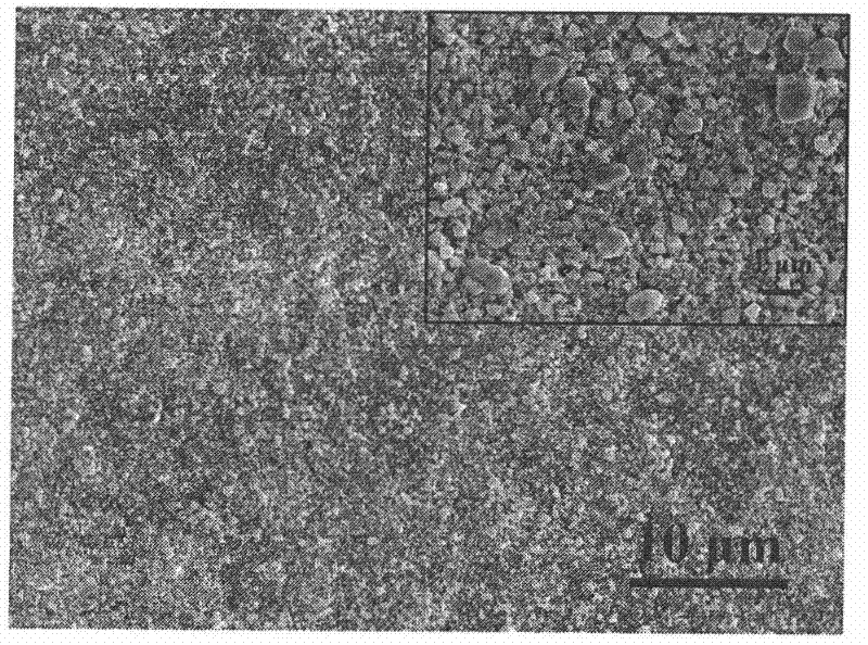
[0027] Immerse the cleaned monocrystalline silicon wafer in the silver coating solution prepared above, react at 50°C for 1.5 hours, then wash with water, and dry to obtain a silver coating composed of nanoparticles on the surface of the monocrystalline silicon wafer (see figure 1 ), the thickness of the coating is 5 μm, and the diameter of the nanoparticles is 100-200 nm.

Embodiment 2

[0029] Weigh the reagent according to the following formula: AgNO 3 3.40 grams, 1.9 grams of NaF, the above reagents were dissolved with a small amount of water respectively, and then mixed and diluted to 1 liter to obtain the silver coating solution of the present invention.

[0030] Wash the (001) oriented monocrystalline silicon wafer with sodium fluoride aqueous solution (concentration: 40 g / L, temperature: 50°C), and then wash with water to remove oxides on the surface of the silicon substrate;

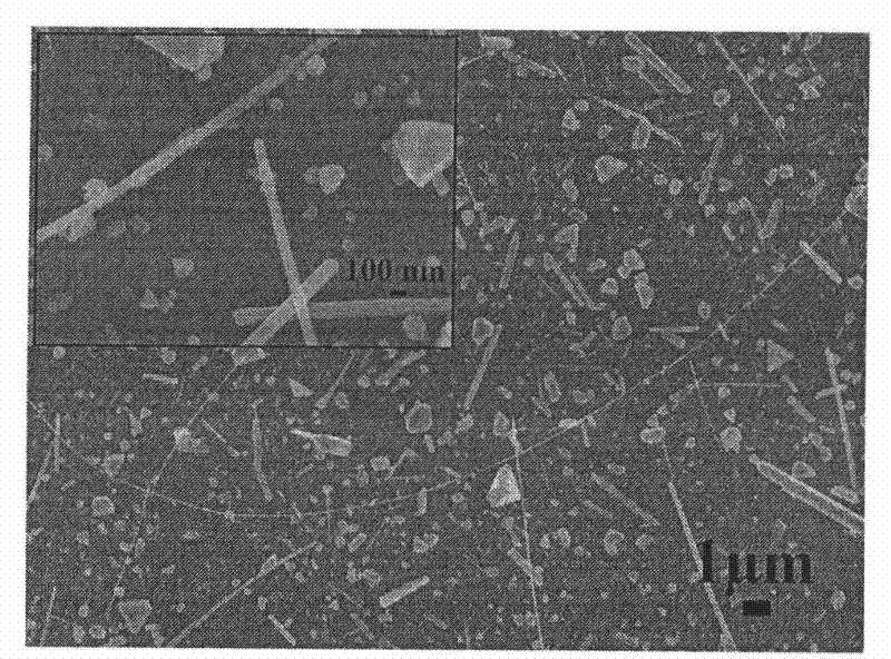
[0031] Dip the cleaned monocrystalline silicon wafer into the silver coating solution prepared above, react at 40°C for 3 hours, then wash with water and dry to obtain a mixed silver coating composed of nanowires and nanoparticles on the surface of the monocrystalline silicon wafer (See figure 2 ), the coating thickness is 80nm, the diameter of the silver nanowire is 40-100nm, and the length is 1-50μm; the diameter of the silver nano-particle is 10-50nm.

Embodiment 3

[0033] Weigh the reagent according to the following formula: AgNO 3 4.5 grams, NaF0.8 grams, PVP (molecular weight 55000) 0.5 grams, above-mentioned reagent is dissolved with a small amount of water respectively earlier, then mixed and diluted to 1 liter, promptly obtains the silver coating solution of the present invention.

[0034] Wash the (001) oriented monocrystalline silicon wafer with sodium fluoride aqueous solution (concentration: 40 g / L, temperature: 50°C), and then wash with water to remove oxides on the surface of the silicon substrate;

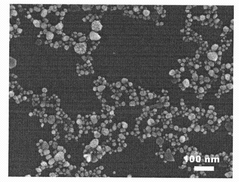
[0035] Dip the cleaned monocrystalline silicon wafer in the silver coating solution prepared above, react at 60°C for 1 hour, then wash with water, and dry to obtain a nanoparticle silver coating on the surface of the monocrystalline silicon wafer (see image 3 ), the thickness of the coating is 20nm, and the diameter of silver nanoparticles is about 10-30nm.


PUM

PropertyMeasurementUnit
thicknessaaaaaaaaaa
diameteraaaaaaaaaa
thicknessaaaaaaaaaa

Abstract

The invention discloses solution for replacing silver plating in deposited nanostructure on the surface of silicon matrix. Water is used as the solvent and each litre of solution contains 3-5 g of AgNO3, 0.5-2.5 g of NaF and 0-100 g of polyvinylpyrrolidone with the molecular weight of 55000. The method for plating a silver layer on the surface of the silicon matrix comprises the following steps of: dipping the cleaned silicon matrix in the silver plating solution at a reaction temperature of 40-60 DEG C, washing with water after depositing and drying to obtain the silver plating in nanostructure on the surface of the silicon matrix, wherein the layer mixed with nanowire and nanoparticles can be obtained when PVP is not contained in the silver plating solution and the nanoparticle layer is obtained when PVP is contained in the silver plating solution. The invention has the advantages of simple component of the solution, gentle reaction as well as simple and controllable plating process, is beneficial to large-scale production and can be used in the production field of very-large-scale integrated circuits and micro electro-mechanical systems.

Description

technical field [0001] The invention relates to a solution for obtaining a silver plating layer on the surface of a silicon substrate, especially a solution for obtaining a nanostructure silver plating layer on the surface of a silicon substrate and a method for using the same. Background technique [0002] Displacement or electroless deposition of metal coatings on silicon substrates is widely used in manufacturing fields such as ultra-large-scale integrated circuits (ULSI) and micro-electromechanical systems (MEMS). Aluminum (with a resistivity of 1.68 μΩcm) and copper (with a resistivity of 2.65 μΩcm) are currently commonly used metallic materials. However, with the increasing integration of integrated circuits and micro-electro-mechanical systems, the metal coating on the surface of silicon wafers requires better electrical conductivity and physical and chemical properties. Compared with other metals, metallic silver does not diffuse into the silicon matrix and has a lo...

Claims


Application Information

Patent Timeline
Patent Type & Authority Patents(China)
IPC IPC(8): C23C18/42C23C18/18
Inventor 谷长栋王秀丽邬震泰涂江平
Owner ZHEJIANG UNIV
Learn More