Process for producing printed wiring board and printed wiring board produced by the production process
A technology for printed wiring substrates and manufacturing methods, applied in the fields of printed circuit manufacturing, printed circuits, printed circuits, etc., can solve the problems of copper wiring short circuit, high insulation resistance, etc., and achieve high insulation reliability and great effect
- Summary
- Abstract
- Description
- Claims
- Application Information
AI Technical Summary
Problems solved by technology
Method used
Image

Examples
Embodiment 1~6、 comparative example 1~6
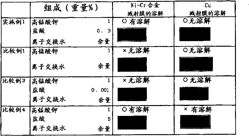
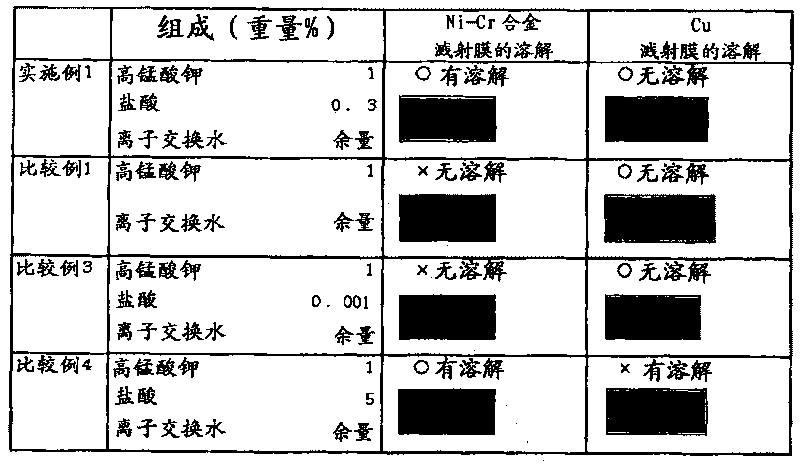
[0093] Hereinafter, examples and comparative examples of the present invention will be described in more detail.
[0094] The Ni-Cr alloy film in embodiment 1~6, comparative example 1~6 is to use 20% by weight Cr-Ni alloy target (Sumitomo Metal Mining Co., Ltd.) was formed with a thickness of 20 to 30 nm by a direct current sputtering method (sputtering device: manufactured by Hirano Koson Co., Ltd.).
[0095] In addition, the copper films in Examples 1 to 6 and Comparative Examples 1 to 6 were formed on the polyimide film in the range of 100 to 120 nm by the DC sputtering method.
[0096] In each of the Examples and Comparative Examples, a predetermined alloy film, metal film, or copper film was individually formed on the polyimide film, and used to evaluate the dissolution of the alloy film, metal film, or copper film respectively. characteristic.
[0097] Potassium permanganate was dissolved in ion-exchanged water with the composition shown in the table below to prepare a...
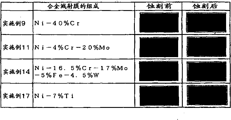
Embodiment 7
[0109] A polyimide film (manufactured by Toray-DuPont Co., film thickness 50 μm) was cut out to a size of 12 cm×12 cm, and a 7% by weight Cr-Ni alloy target (manufactured by Sumitomo Metal Mining) was used on one side, and was sputtered by direct current A 7% by weight Cr—Ni alloy metal film was formed with a thickness of 20 to 30 nm using a sputtering apparatus: manufactured by Hirano Koson Co., Ltd. An evaluation sample of 50 mm x 50 mm was cut out from the obtained polyimide film forming an alloy film, and was heated at 40° C. After dipping for 2 minutes, the degree of dissolution of the alloy film was visually confirmed, and the dissolution of the alloy film was observed.
Embodiment 8
[0111] In the same manner as in Example 7, a 30 wt% Cr-Ni alloy metal film was formed by the DC sputtering method using a 30 wt% Cr-Ni alloy target (manufactured by Sumitomo Metal Mining Co., Ltd.). An evaluation sample of 50 mm x 50 mm was cut out from the obtained polyimide film forming an alloy film, and was heated at 40° C. After dipping for 2 minutes, the degree of dissolution of the alloy film was visually confirmed, and the dissolution of the alloy film was observed.
PUM
 Abstract
Description
Claims
Application Information
 - R&D
- Intellectual Property
- Life Sciences
- Materials
- Tech Scout
- Unparalleled Data Quality
- Higher Quality Content
- 60% Fewer Hallucinations
Browse by: Latest US Patents, China's latest patents, Technical Efficacy Thesaurus, Application Domain, Technology Topic, Popular Technical Reports.
© 2025 PatSnap. All rights reserved.Legal|Privacy policy|Modern Slavery Act Transparency Statement|Sitemap|About US| Contact US: help@patsnap.com