Method for manufacturing shallow trench isolation structure

A technology of isolation structure and manufacturing method, which is applied in the field of manufacturing shallow trench isolation structures, can solve problems such as increased stress and affecting the quality of lining oxide layers, and achieve the effects of releasing stress, short irradiation time, and improving quality

Inactive Publication Date: 2010-06-09
SEMICON MFG INT (SHANGHAI) CORP
View PDF1 Cites 6 Cited by
  • Summary
  • Abstract
  • Description
  • Claims
  • Application Information

AI Technical Summary

Problems solved by technology

[0008] In the existing process of forming a shallow trench isolation structure, since the etching gas or liquid will generate defects on the inner wall of the shallow trench when etching to form the shallo

Method used


Image

  • Method for manufacturing shallow trench isolation structure
  • Method for manufacturing shallow trench isolation structure
  • Method for manufacturing shallow trench isolation structure

Examples


Example Embodiment

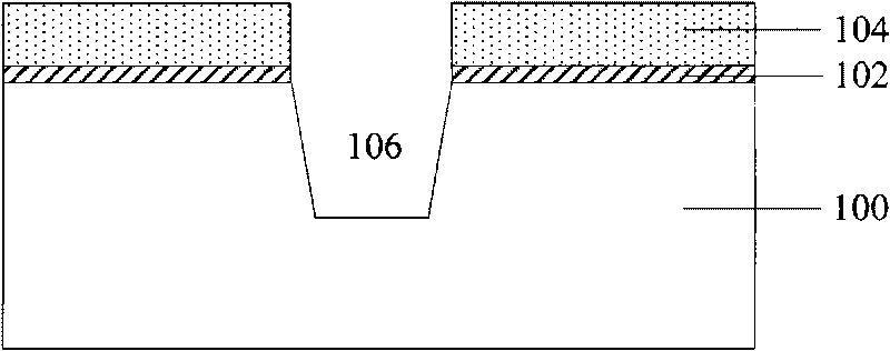
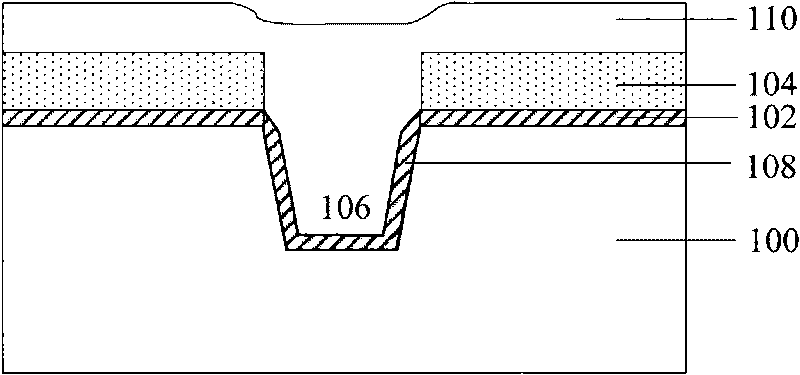
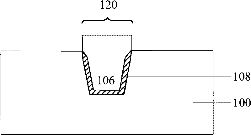
[0020] In the process of forming the shallow trench isolation structure in the prior art, when the shallow trench is formed by etching, the etching gas or liquid will react with the semiconductor substrate in the shallow trench to form defects, or produce defects on the surface of the semiconductor substrate. Residual, if not repaired, it will affect the quality of the lining oxide layer formed later, and cause leakage current phenomenon at the corners of the shallow trench. In addition, after the shallow trench is formed, the semiconductor substrate therein is easily oxidized by oxygen or water vapor when exposed to the air, forming a native oxide layer, which is poor in density and uniformity. In order to solve the above problems, the present invention uses a laser to heat the inner wall of the shallow trench before forming the lining oxide layer. Due to the high intensity and short time of the laser, the defects on the semiconductor substrate can be repaired in time and the o...


PUM

PropertyMeasurementUnit
Laser poweraaaaaaaaaa
Thicknessaaaaaaaaaa

Abstract

The invention provides a method for manufacturing a shallow trench isolation structure. The method comprises the following steps: forming a pad oxide layer and a corrosion barrier layer on a semiconductor substrate in sequence; etching the corrosion barrier layer, the pad oxide layer and the semiconductor substrate to form a shallow trench; carrying out laser heat treatment on the semiconductor substrate in the shallow trench, and introducing oxygen into the substrate to form a lining oxide layer; filling insulating oxide layers in the shallow trench; removing the corrosion barrier layer and the pad oxide layer until the semiconductor substrate is exposed so as to form the shallow trench isolation structure. The method improves the quality of the subsequent lining oxide layer, reduces leakage current, and improves the quality of semiconductor devices.

Description

technical field [0001] The invention relates to the manufacturing field of semiconductor devices, in particular to a manufacturing method of a shallow trench isolation structure. Background technique [0002] As the size of integrated circuits decreases, the devices that make up the circuits must be placed more densely to fit the limited space available on the chip. Since current research is devoted to increasing the density of active devices per unit area of ​​a semiconductor substrate, effective insulating isolation between circuits becomes more important. The methods for forming isolation regions in the prior art mainly include local oxidation isolation (LOCOS) process or shallow trench isolation (STI) process. The LOCOS process is to deposit a layer of silicon nitride on the surface of the wafer, and then perform etching to oxidize and grow silicon oxide in part of the recessed area, and the active device is generated in the area determined by the silicon nitride. For ...

Claims


Application Information

Patent Timeline
IPC IPC(8): H01L21/762
Inventor 王津洲高大为
Owner SEMICON MFG INT (SHANGHAI) CORP
Why Eureka
Try Eureka