Fabrication method for crystalline semiconductor films on foreign substrates

a technology of crystalline semiconductor and foreign substrate, which is applied in the field of fabrication method of crystalline semiconductor films on foreign substrates, can solve the problems of limited thermal stability of commercially available low-cost glass substrates, limited thermal budget of each fabrication step, and inability to meet the requirements of manufacturing, etc., and achieves the effect of reducing the minimum tim

Inactive Publication Date: 2006-11-09
NEWSOUTH INNOVATIONS PTY LTD
View PDF2 Cites 31 Cited by
  • Summary
  • Abstract
  • Description
  • Claims
  • Application Information

AI Technical Summary

Benefits of technology

[0034] If instead of an aluminium hydroxide film an aluminium oxide film is grown, the surface of the aluminium layer is exposed to a dry air atmosphere (0% relative humidity) for at least 6 hours at room temperature (i.e. 22°±1°) and a pressure of 1 atmosphere. As with hydroxide films, the process slows down as the film grows and is essentially self limiting so that there is no upper limit to the useful time of exposure. A period of 24 hours is usually employed. Again increasing the temperature while the oxide film is growing will decrease the minimum time required.
[0035] If formin...

Problems solved by technology

However the limited thermal stability of commercially available low-cost glass substrates severely limits the allowable thermal budget of each fabrication step (as a rule of thumb, the glass temperature must not exceed 650° C. if the process lasts 1 hour or more), resulting in the need for a new technology enabling good material quality at these low temperatures.
Such fine-grained (<500 nm) material is inevitably of rather low electronic quality.
A drawback of the hydrogen-diluted PECVD approach with regard to the manufacture of devices that require a rather thick semiconductor film (such as crystalline silicon solar cells) is the low deposition rate for nanocrystalline semiconductor material (much less than 1 nm/s in the case of Si).
Compared to nanocrystalline material, polycrystalline material theoretically has a much better electronic quality, however achieving good-quality polycrystalline material at low temperature on a foreign substrate has proven difficult to achieve.
All of the methods mentioned above have been limited by one or more of the following factors: i. long processing times, ii. rough surfaces, iii. highly doped films iv. small grain siz
Despite a high level of research interest, none of them has as yet led to a commercially available photovoltaic device.
However, with respect to using the resulting polycrystalline semiconductor film for the fabrication of electronic devices or as seed layer, a significant problem of the MIC-prepared polycrystalline semico...

Method used


Image

  • Fabrication method for crystalline semiconductor films on foreign substrates
  • Fabrication method for crystalline semiconductor films on foreign substrates
  • Fabrication method for crystalline semiconductor films on foreign substrates

Examples


Embodiment Construction

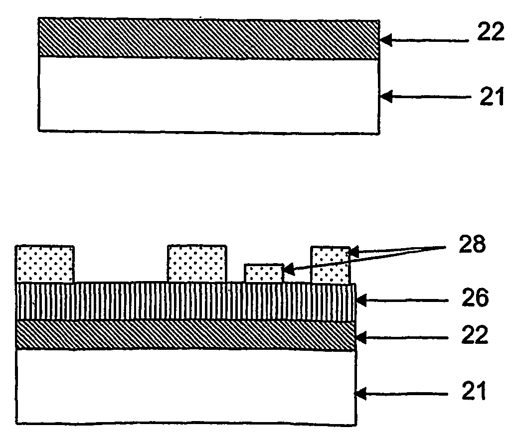
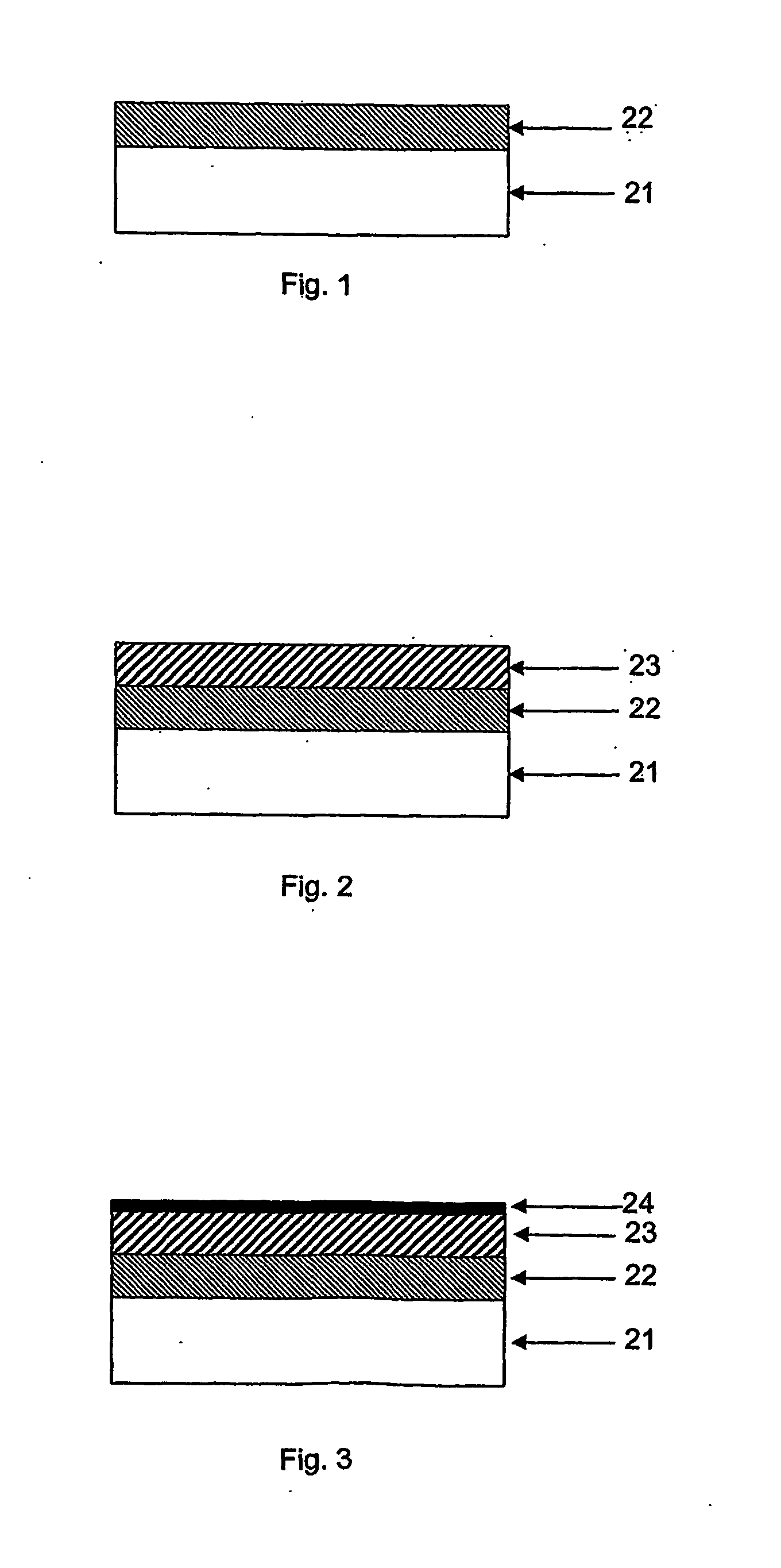
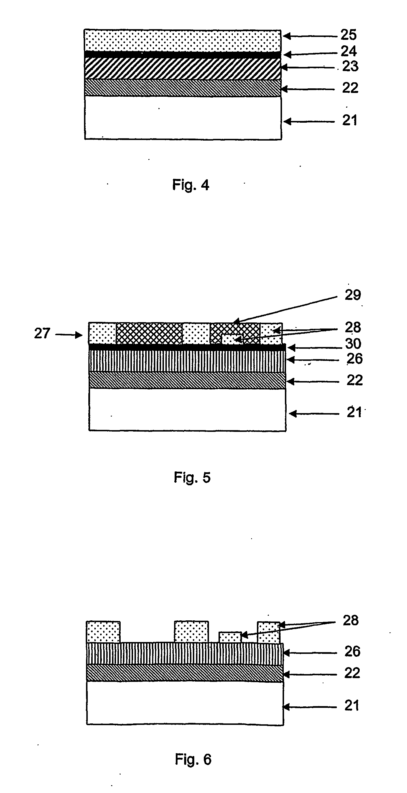
[0078] An embodiment of the invention will now be described which has demonstrated an ability to produce large-grained, island-free polycrystalline silicon with arbitrary doping on planar glass substrates. However, while the process is described for a silicon film on a glass substrate it will be appreciated that the process is also applicable to other semiconductors and foreign substrates.

[0079] The formation of a device-quality polycrystalline silicon layer on glass is a two-step process, the first of which is to form a high-quality seed layer and the second is to form the device-grade layer over the seed layer. The formation of the seed layer involves the low-temperature (≦650° C.) formation of a polycrystalline semiconductor film on a supporting substrate by means of metal-induced crystallisation (MIC) of amorphous films of the same semiconductor material and is schematically shown in FIGS. 1 and 6. The metal and semiconductor must be chosen such that they can form an eutectic s...


PUM


Abstract

The invention provides a method of forming a polycrystalline semiconductor film on a supporting substrate of foreign material. The method involves depositing a metal film onto the substrate, forming a film of metal oxide and/or hydroxide on a substrate of the metal, and forming a layer of an amorphous semiconductor material over a surface of the metal oxide and/or hydroxide film. The entire sample is then heated to a temperature at which the semiconductor layer is absorbed into the metal layer and deposited as a polycrystalline layer onto the target surface by metal-induced crystallization. The metal is left as an overlayer covering the deposited polycrystalline layer, with semiconductor inclusions in the metal layer. The polycrystalline semiconductor film and the overlayer are generated by porous interfacial metal oxide nd/or hydroxide film. The metal in the overlayer and the interfacial metal oxide and/or hydroxide film are then removed with an etch which underetches the semiconductor inclusions to form freestanding islands. Finally, the freestanding semiconductor “islands” are removed from the surface of the polycrystalline semiconductor layer by a lift-off process.

Description

INTRODUCTION [0001] The present invention relates generally to the formation of thin semiconductor films for electronic device fabrication, and in particular the invention provides a method for the formation of thin polycrystalline semiconductor films on foreign substrates, using a thermal budget in each process step that is compatible with the respective foreign substrate. Throughout this text, the term polycrystalline material means material that has an average crystal grain size of above 500 nm and the term thermal budget relates to the amount of heat applied during a process step (i.e., the area below the temperature-time curve of the process step). BACKGROUND OF THE INVENTION [0002] Thin films of polycrystalline silicon (pc-Si) on glass or other foreign substrates are very attractive for a wide range of large-area electronic applications, including thin-film photovoltaic (PV) modules, active matrix liquid crystal displays (AMLCDs), and active matrix organic light emitting diode...

Claims


Application Information

Patent Timeline
IPC IPC(8): H01L21/20H01L21/36H01L31/18
CPCH01L21/2022Y02E10/546H01L31/182Y02P70/50H01L21/02425H01L21/02422H01L21/02488H01L21/02532H01L21/0242H01L21/02672H01L21/02667H01L21/02639
Inventor ABERLE, ARMIN GERHARDWIDENBORG, PER INGEMARSTRAUB, AXELNEUHAUS, DIRK-HOLGERHARTLEY, OLIVERHARDER, NILS-PETER
Owner NEWSOUTH INNOVATIONS PTY LTD
Why Eureka
Try Eureka