Flip chip bonding process for base plate

A flip-chip and substrate technology, which is applied in the manufacture of electrical components, electrical solid devices, semiconductor/solid devices, etc., can solve problems such as poor stability, difficult process control, poor contact between solder joints and substrate pads, and welding strength. Good process stability, improved interconnection yield, and high soldering strength

Inactive Publication Date: 2010-06-16
SHANGHAI INST OF MICROSYSTEM & INFORMATION TECH CHINESE ACAD OF SCI
View PDF0 Cites 10 Cited by
  • Summary
  • Abstract
  • Description
  • Claims
  • Application Information

AI Technical Summary

Problems solved by technology

The traditional flip-chip soldering process has high requirements on the coplanarity of the chip solder joints, the process is difficult to control, and the stability is poor. The conduction rate of the flip-chip soldered interconnect components obtained is not high, and there is poor contact between the solder joints and the substrate pads. And the problem of low soldering strength [1.Xiao G W, Chan P C

Method used


Image

  • Flip chip bonding process for base plate
  • Flip chip bonding process for base plate

Examples


Embodiment Construction

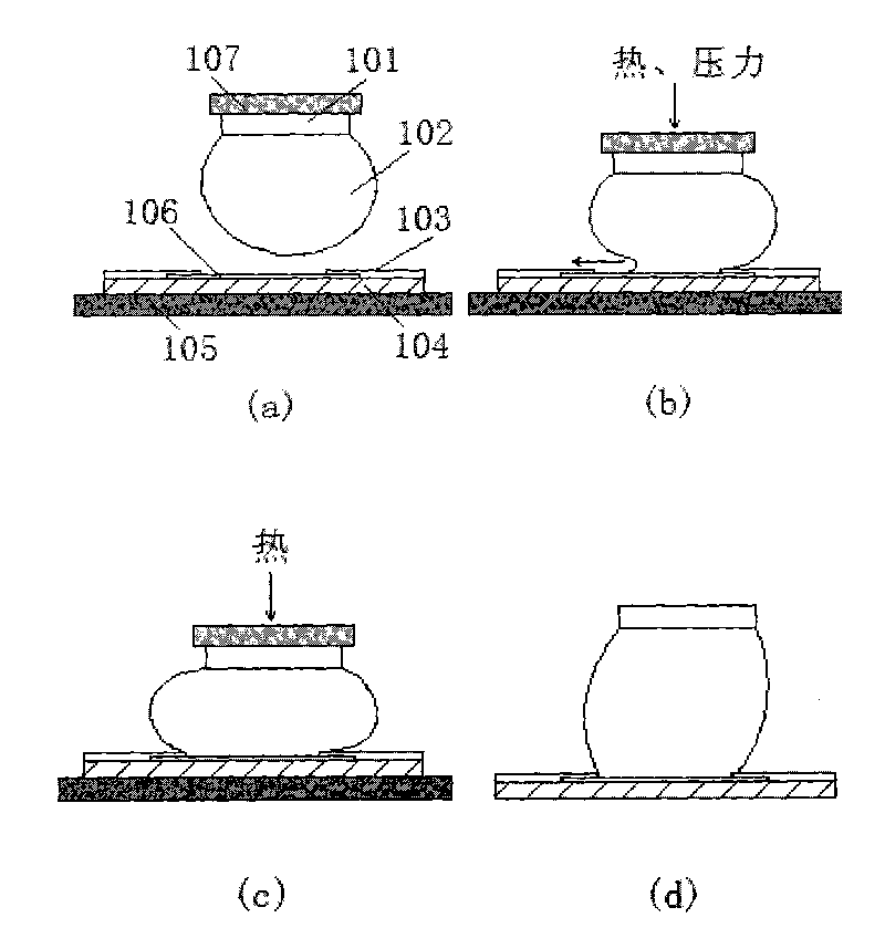
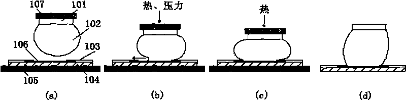
[0012] The substantive features and remarkable progress of the substrate flip-chip welding process provided by the present invention will be further described below in conjunction with the accompanying drawings, but the present invention is by no means limited to the embodiments.

[0013] The large deformation preloaded substrate flip-chip welding process of the present invention comprises the following steps:

[0014] (1) heating the substrate 104 and the chip 101 to 50°C-200°C by heating the flip-chip welding machine base 105 and the chip suction head 107;

[0015] (2) Print flux on the printed circuit substrate 104, such as the RF800 of Alpha Company, and place the substrate on the flip-chip soldering machine base 105, and place the chip bumps after scribing on the carrier sheet facing down On the stage, utilize the vacuum suction head 107 to pick up the chip 101 from the back ( figure 1 (a));

[0016] (3) utilize beam splitter to carry out chip bump 102 and the welding p...


PUM


Abstract

The invention relates to a flip chip bonding process for a large-deformation pre-pressed base plate. The process is characterized in that: firstly, a soldering flux is printed on the base plate; after the soldering flux is coated and a chip is aligned with the base plate, certain pre-pressure is applied to one side of a suction head at a chip end, so that salient points undergo large deformation under the pre-pressure and is tightly connected with a Cu soldering-pan on a PCB in a more effective mode; and the height of a welding spot is recovered under the effect of surface tension in a subsequent refluxing process. The interconnection rate between a high-density welding spot and a PCB base plate is greatly enhanced, basically to 100 percent, and reliable interconnection between the welding spot and the PCB base plate can also be realized even under the condition of poor coplanarity of array salient points or severe alignment error between the welding spot and the Cu soldering-pan. The process solves the problem of low conduction rate between the high-density salient points and the soldering-pan, and has the advantages of high welding intensity, good technical stability and high repeatability.

Description

technical field [0001] The invention relates to a substrate flip-chip welding process, more precisely relates to a substrate flip-chip welding process with large deformation and preloading, and belongs to the field of electronic packaging. Background technique [0002] The traditional flip-chip soldering process first prints flux on the substrate, and the flux plays a role in fixing the chip on the pad position before reflow, and plays a role in reducing oxidation during reflow. After the flux is printed, the substrate is placed on the base of the flip-chip welding machine, and the diced chip bump is placed on the carrier table, and the chip is picked up from the back by the vacuum suction head, and the bump is carried out by using the beam splitter. After alignment with the pads on the substrate, the suction head mounts the chip solder balls on the pads of the substrate. In addition to paying attention to the alignment of the solder ball and the pad when mounting the chip,...

Claims


Application Information

Patent Timeline
IPC IPC(8): H01L21/603
CPCH01L24/81
Inventor 林小芹罗乐
Owner SHANGHAI INST OF MICROSYSTEM & INFORMATION TECH CHINESE ACAD OF SCI
Why Eureka
Try Eureka