
Device and method for arranging a plurality of cells at same plane and controlling cells

A cell and unified technology, applied in tissue cell/virus culture devices, biochemical equipment and methods, biochemical instruments, etc., can solve the problems of limited price application, expensive absorption of gold flakes, lack of elasticity of gold flakes, etc.

Active Publication Date: 2010-06-23
重庆龙翼生物科技有限公司
View PDF0 Cites 8 Cited by
  • Summary
  • Abstract
  • Description
  • Claims
  • Application Information

AI Technical Summary

Problems solved by technology

However, this method can only arrange cells on the surface of the gold sheet, and the gold sheet has no elasticity, and the absorption of fluorescence by the gold sheet and its high price limit its application.

Method used


Image

  • Device and method for arranging a plurality of cells at same plane and controlling cells
  • Device and method for arranging a plurality of cells at same plane and controlling cells
  • Device and method for arranging a plurality of cells at same plane and controlling cells

Examples


Embodiment 1

[0063] 1) Preparation of polydimethylsiloxane stamp:

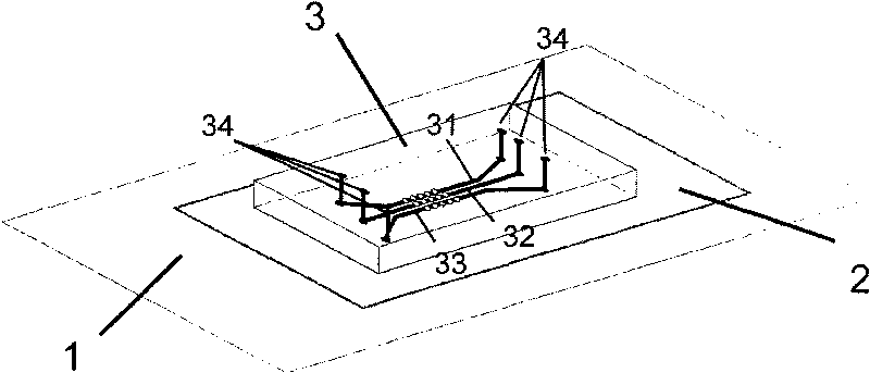
[0064] Use photolithography to prepare at least one group of convex linear microstructure units on a silicon wafer (the present embodiment figure 1 shown three convex lines), first use the drawing software L-edit to design the desired graphics: three convex line bands (the middle convex line band at the middle position, and the convex line bands located on both sides of the middle convex line band respectively) side convex lines), the length of the convex lines is 1.2 cm, the middle sections of the convex lines on both sides are respectively parallel to the middle convex lines, and the middle sections of the convex lines on both sides are The two ends outside are inclined away from the direction of the middle convex line (the length is 0.5 cm, whose length is this?), the interval between the two convex lines is 200 microns, and each convex line The tape width is 400 microns;

[0065] Using the above-mentioned silicon chi...

Embodiment 2

[0080] 1) Use photolithography to prepare at least one set of convex linear microstructure units on the silicon wafer, first use the graphics software L-edit to design the desired pattern: three parallel convex lines and a circular array of convex structures , the length of the three convex strips is 1.2 cm, the outer two ends are inclined outwards, the length is 0.5 cm, the middle part is parallel, the distance between each other is 200 microns, and the width of each strip is 400 microns. The circular micro-column array has three columns with a diameter of 300 microns and a height of 100 microns, each column has ten micro-columns, and the interval between each column is 300 microns, and the space between the columns in each column is also 300 microns.

[0081] 2) Flipping the convex linear microstructure unit obtained in step 1) with polydimethylsiloxane (PDMS) to obtain a PDMS stamp with a concave pattern corresponding to the above microstructure.

[0082] 3) Spread unpolyme...

Embodiment 3

[0090] 1) Use photolithography to prepare at least one set of convex linear microstructure units on the silicon wafer, first use the graphics software L-edit to design the desired pattern: three parallel convex lines and a circular array of convex structures , the length of the three convex strips is 1.2 cm, the outer two ends are inclined outward, the length is 0.5 cm, the middle part is parallel, and the distance between each other is 200 microns, the width of the first and second strips is 400 microns, and the width of the third strip is 1 mm. The circular micropillar array is three columns, with a diameter of 300 microns and a height of 100 microns, with four microcolumns in each column, such as figure 2 As shown, the interval between each column is 300 microns, and the interval between the columns is also 300 microns. The interval between the first two columns of the third column and the second column is 300 microns, and the interval between the last two columns and the ...


PUM

PropertyMeasurementUnit
Lengthaaaaaaaaaa
Lengthaaaaaaaaaa
Diameteraaaaaaaaaa

Abstract

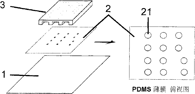
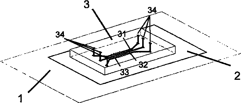
The invention discloses a device and a method for arranging a plurality of cells at the same plane and controlling the cells, comprising: a thin film with micro-hole arrays which is located at the upper surface of a base; a PDMS stamp whose lower surface is provided with a micro-groove unit and is coated on the thin film; the micro-groove unit comprises: an intermediate groove and a left-side groove and a right-side groove which are located at the left side and the right side of the intermediate groove; the middle sections of the left-side groove and the right-side groove are parallel to the intermediate groove; the both end sections except for the middle sections of the left-side groove and the right-side groove slant towards the direction away from the intermediate groove; the end of the groove is provided with a vertical through hole which is communicated with the corresponding groove; the holes of the thin film are all located in the micro-groove of the stamp; and a micro-pipeline is provided with different cell suspensions, the cell grows in the micro-pipeline and adheres to the micro-pipeline; the stamp is removed to realize the co-culture of a plurality of cells at the same plane; and then the thin film is removed to realize the free movement of the plurality of co-cultured cells at the same plane; the method is simple to operate, the used material is cheap, and the invention can be used for high-throughput screening of useful drugs for cells.

Description

technical field [0001] The invention belongs to the device and method for arranging multiple cells on the same plane and manipulating them, belonging to the field of biotechnology. Background technique [0002] Accurately arranging a variety of cells on the same plane not only plays a wide role in basic biology, such as the study of cell migration and cell interaction, but also provides a platform for tissue engineering and drug screening. Scientists have developed some related methods: [0003] For example, Document 1: Chui, D.T.et al.Proc.Natl.Acad.Sci.U.S.A.2000, 97, (6), 2408-2413, the Whitesides group of Harvard University, using a PDMS microfluidic channel with a three-dimensional structure, on the same surface Array of various cells. This method first makes a PDMS "stamp" with a three-dimensional structure. After the "stamp" is combined with the substrate for culturing cells, different kinds of cells are introduced into the microfluidic channel, so that the cells wi...

Claims


Application Information

Patent Timeline
IPC IPC(8): C12M3/00C12N5/00
Inventor 蒋兴宇袁博李勇
Owner 重庆龙翼生物科技有限公司
Learn More