Semiconductor high-voltage terminal structure and production method thereof

A terminal structure and manufacturing method technology, which is applied in semiconductor/solid-state device manufacturing, semiconductor devices, semiconductor/solid-state device components, etc., can solve the problems of slow gradient gradient, cumbersome process, and complex calculation, etc., and achieve downsizing , Improve the effect of process tolerance

Active Publication Date: 2010-06-23
商海涵
View PDF7 Cites 27 Cited by
  • Summary
  • Abstract
  • Description
  • Claims
  • Application Information

AI Technical Summary

Problems solved by technology

However, this method needs to calculate the number and density of channels in advance according to the proposed impurity distribution gradient. Such calculation is relatively complicated, and the calculation process needs to be simulated and continuously corrected. The process is cumbersome.
In addition, the impurity gradient obtained through channel arrangement is obviously jagged, and cannot reach a relatively continuous gradient.

Method used


Image

  • Semiconductor high-voltage terminal structure and production method thereof
  • Semiconductor high-voltage terminal structure and production method thereof
  • Semiconductor high-voltage terminal structure and production method thereof

Examples


Embodiment Construction

[0023] Specific embodiments of the present invention will be described in detail below in conjunction with the accompanying drawings.

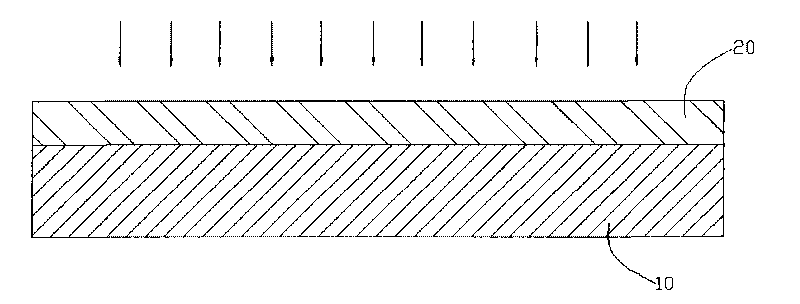
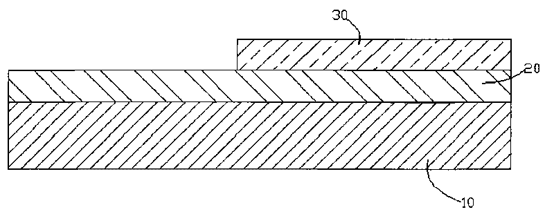
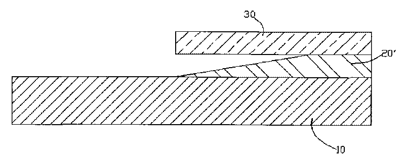
[0024] Please refer to figure 1 , the first step of the manufacturing method of the semiconductor high-voltage terminal structure of the present invention is to form a field oxide layer 20 by thermal growth on the silicon (Si) substrate 10, and the field oxide layer 20 is silicon dioxide (SiO 2 ) layer with a thickness of 1000 nm-1500 nm, in fact, the field oxide layer can also be other silicon compounds, such as silicon oxynitride and the like. By means of ion bombardment, a damaged layer is introduced on the top of the field oxide layer, so that this part of the damaged field oxide layer has a faster corrosion rate; this effect can also be achieved by chemical vapor deposition of a certain thickness of corrosion-prone oxide layer is reached. In this step, in order to corrode the field oxide layer into a slope shape in subsequent steps, it ...


PUM


Abstract

The invention provides a semiconductor high-voltage terminal structure and a production method thereof. The method comprises the steps of: firstly providing a silicon baseplate, forming a field oxide layer on the silicon baseplate and introducing an easily corroded layer in the field oxide layer; identifying a high-voltage terminal structure area by using a photomask; and then corroding the fieldoxide layer by using a wet method to form a ramp oxide layer with an oblique angle; carrying out ion implantation by using the ramp oxide layer as a self-aligned mask to introduce initial impurities diffusing horizontally; and finally forming a high-voltage protection ring with a horizontal doping gradient at the starting end of the ramp oxide layer; and forming a ramp field plate by depositing high-doping polycrystalline silicon or metal on the ramp oxide layer. The semiconductor high-voltage terminal structure comprises the silicon baseplate, the ramp oxide layer arranged on the silicon baseplate, the high-voltage protection ring with a horizontal doping gradient which is injected by taking the ramp oxide layer as the self-aligned mask, and the high-doping polycrystalline silicon or metal ramp field plate deposited on the ramp oxide layer.

Description

technical field [0001] The invention relates to a method for manufacturing a semiconductor, in particular to a method for manufacturing a semiconductor high-voltage terminal structure, and to a semiconductor high-voltage terminal structure obtained by the method. Background technique [0002] Field plates and field limiting rings are common terminal protection technologies used to improve the ability of semiconductor components to withstand voltage breakdown. In high-voltage devices, the high-voltage terminal protection ring structure with gradual lateral doping gradient (VLD) is generally considered to be more Uniformly doped field limiting rings have higher efficiency. [0003] Usually, the graded lateral doping gradient high-voltage termination structure related to the present invention is fabricated using a mask. A number of strip-shaped and hole-shaped channels are set on the mask plate, and these channels are used as ion implantation windows, and the required lateral ...

Claims


Application Information

Patent Timeline
Patent Type & Authority Applications(China)
IPC IPC(8): H01L21/00H01L23/00
Inventor 龚大卫邵凯
Owner 商海涵
Why Eureka
Try Eureka