Chip scale package structure of CMOS (complementary metal-oxide-semiconductor) image sensor and packaging method

A chip-level packaging and image sensor technology, which is applied in the semiconductor field, can solve the problems of a large number of connecting wires, affecting the freedom of connecting wire layout, and failing to meet device integration, so as to reduce defect dislocations and improve efficiency.

Active Publication Date: 2010-06-23
SEMICON MFG INT (SHANGHAI) CORP
View PDF1 Cites 12 Cited by
  • Summary
  • Abstract
  • Description
  • Claims
  • Application Information

AI Technical Summary

Problems solved by technology

For high-pixel CMOS sensors, the number of connection lines is huge, and the use of solder technology not only affects the freedom of the entire conne

Method used


Image

  • Chip scale package structure of CMOS (complementary metal-oxide-semiconductor) image sensor and packaging method
  • Chip scale package structure of CMOS (complementary metal-oxide-semiconductor) image sensor and packaging method
  • Chip scale package structure of CMOS (complementary metal-oxide-semiconductor) image sensor and packaging method

Examples


no. 1 approach

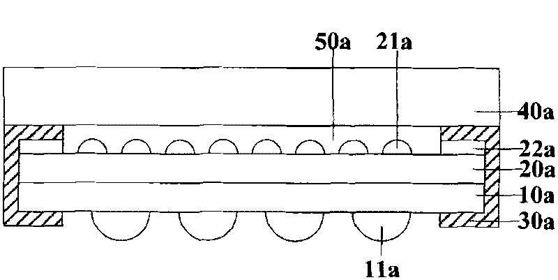
[0016] The first embodiment of the present invention provides a chip-level packaging method for a CMOS semiconductor image sensor, including: providing a semiconductor substrate, forming a photoelectric conversion layer in the semiconductor substrate, and forming a wiring layer on the surface of the photoelectric conversion layer. A discrete connection pad is formed on the surface; an adhesion layer is formed on the surface of the wiring layer, and the adhesion layer covers the connection pad; a support layer is formed on the surface of the adhesion layer; the semiconductor substrate is thinned until the photoelectric conversion layer is exposed, the photoelectric conversion layer An array of pixel elements and a connection layer between the pixel elements are formed thereon, the connection layer is higher than the pixel elements; an adhesive layer is formed on the surface of the microlens layer and the surface of the connection layer; a light-transmitting layer is formed on the ...

no. 2 approach

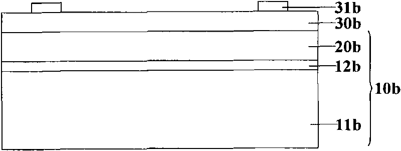
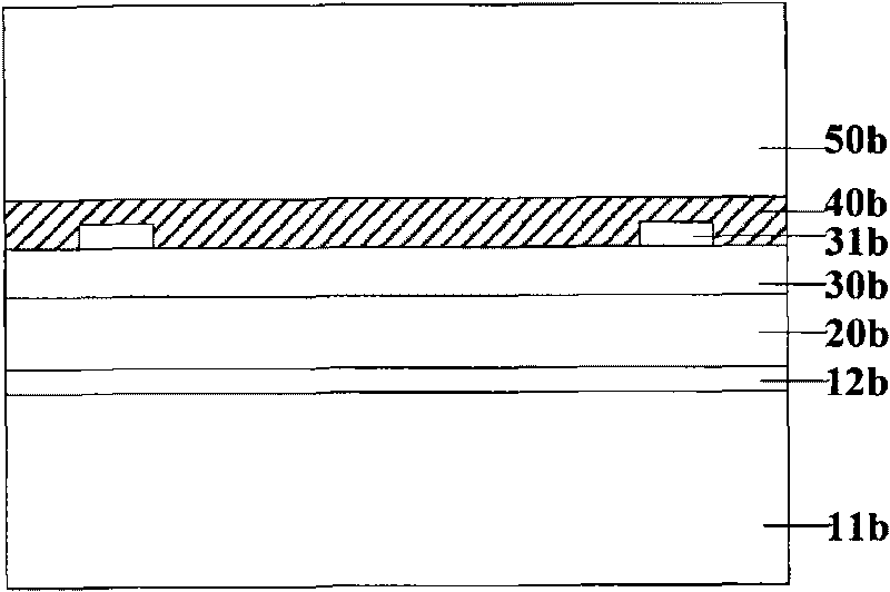
[0040] The first embodiment of the present invention provides a chip-scale packaging method for a CMOS semiconductor image sensor, including providing a semiconductor substrate, forming a photoelectric conversion layer in the semiconductor substrate, and forming a wiring layer on the surface of the photoelectric conversion layer. A discrete connection pad is formed on the surface; an adhesion layer is formed on the surface of the wiring layer, and the adhesion layer covers the connection pad; a support layer is formed on the surface of the adhesion layer; the semiconductor substrate is thinned until the photoelectric conversion layer is exposed, the photoelectric conversion layer An array of pixel elements and a connection layer between the pixel elements are formed thereon, the connection layer is higher than the pixel element; an adhesive layer is formed on the surface of the pixel element and the surface of the connection layer; a light-transmitting layer is formed on the surf...


PUM

PropertyMeasurementUnit
Thicknessaaaaaaaaaa
Thicknessaaaaaaaaaa
Thicknessaaaaaaaaaa

Abstract

The invention discloses a chip scale package structure of a CMOS (complementary metal-oxide-semiconductor) image sensor and a packaging method. The chip scale package structure of the CMOS image sensor comprises a photoelectric conversion layer, a pixel element array, a connection layer, an adhesion layer, a photic zone, a wiring layer, a connection pad, a separating layer, and solder joints, wherein the pixel element array is positioned on the photoelectric conversion layer; the connection layer is positioned on the photoelectric conversion layer for separating the pixel element array and is higher than a pixel element; the adhesion layer is positioned on the surfaces of a micro lens and the connection layer, and the photic zone is positioned on the adhesion layer; the pixel element area forms a cavity; the wiring layer is positioned on the surface opposite to the surface located by the photoelectric conversion layer and the pixel element array; the connection pad is discreted on the wiring layer; the separating layer is positioned on the wiring layer and exposes the connection pad; and the soldering spots are positioned on the connection pad. The invention effectively improves the performance and the integration level of a device.

Description

Technical field [0001] The present invention relates to the field of semiconductor technology, in particular to a chip-level packaging structure and packaging method of a CMOS image sensor. Background technique [0002] At present, charge coupled device (CCD) is the main practical solid-state image sensor device. It has the advantages of low reading noise, large dynamic range, and high response sensitivity. However, CCD also has the advantages of complementary metal oxide semiconductor ( Complementary-Metal-Oxide-Semiconductor (CMOS) technology is compatible, that is, it is difficult to realize single-chip integration for CCD-based image sensors. [0003] CMOS image sensor (CMOS Image sensor, CIS) is produced to overcome the complexity and high energy consumption of charge coupled device (CCD) manufacturing process. CMOS manufacturing technology is applied, and the number corresponds to the number of unit pixels in the semiconductor substrate. MOS transistor. Because CIS adopts C...

Claims


Application Information

Patent Timeline
IPC IPC(8): H01L21/50H01L21/60H01L27/146H01L23/48
CPCH01L2224/10H01L2924/13091
Inventor 三重野文健鲍震雷
Owner SEMICON MFG INT (SHANGHAI) CORP
Why Eureka
Try Eureka