On-wafer self-test and self-repair method

A self-repair and self-test technology, which is applied in the field of integrated circuit testing and integrated circuit design, can solve problems such as increased cost, self-test, and self-repair unit complexity, so as to improve yield and reliability, reduce test cost, and shorten test the effect of time

Active Publication Date: 2010-06-30
SHANGHAI XINHAO MICROELECTRONICS
View PDF14 Cites 14 Cited by
  • Summary
  • Abstract
  • Description
  • Claims
  • Application Information

AI Technical Summary

Problems solved by technology

[0019] To sum up, the existing self-test and self-repair methods either use highly complex algorithms, the self-te...

Method used


Image

  • On-wafer self-test and self-repair method
  • On-wafer self-test and self-repair method
  • On-wafer self-test and self-repair method

Examples


Embodiment Construction
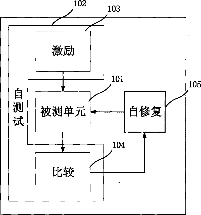
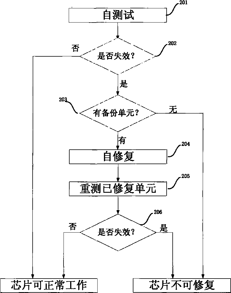
[0055] The technical idea of ​​the invention is to realize the detection and self-repair of the tested unit through the self-test unit and the self-repair unit. Firstly, the self-test unit is used to test whether the unit under test fails, and the test result is passed to the self-repair unit. The self-repair unit uses the backup unit column to replace the failed unit to complete self-repair. Restoration does not require external intervention and complex algorithms.

[0056] see figure 1 , which is a structural diagram of a chip system implementing on-chip self-test and self-repair. The system consists of three parts: a unit under test (101), a self-test unit (102) and a self-repair unit (105). Wherein, the tested unit (101) includes but not limited to logic unit, memory, internal wiring, input and output pins. The self-test unit (102) gives the unit under test (101) an incentive (103), and the output of the unit under test is returned to the self-test unit (102) for compar...


PUM


Abstract

The invention belongs to the field of integrated circuit design, particularly relates to a method capable of carrying out self test on a chip without depending on an external device in the condition of live working and performing self repair according to a test result. The self test of the method can be applied to all structures and parts in the chip; and the self repair of the method can be applied to all structures and parts with backup units. The self-test and self-repair course based on the method comprises two stages: a first stage is test and repair stage, wherein the self test is carried out firstly, and a failure unit is replaced by a backup unit according to a test result; and a second stage is the retest stage, wherein if no error is tested, the on-wafer self-test and self-repair is finished, and otherwise an unrepairable signal is produced for external detection. The invention realizes on-wafer self repair with lower cost and replaces a failure part with the backup unit, thereby improving the yield rate and the reliability of the chip, and effectively reducing the testing time and the testing cost.

Description

technical field [0001] The invention relates to the field of integrated circuit design, in particular to the field of integrated circuit testing. Background technique [0002] With the advancement of technology, in the field of integrated circuit design, the multi-core structure and the integration of more logic units, IP cores, and memories in the SOC system have become a development trend. With the increasing demand for functions and performance, chips There are more and more applications of medium, high-speed and high-bandwidth system buses. The bit width of 32-bit and 64-bit system buses is very common, and the wider 128-bit on-chip bus has also begun to be widely used. Another problem caused by the improvement of system integration is the increase in the number of chip external pins. [0003] In terms of logic unit testing, since there are many units under test, if each unit under test is tested sequentially in a serial order, it will take a long time to test and incre...

Claims


Application Information

Patent Timeline
IPC IPC(8): G11C29/00G11C29/44G01R31/3187H01L21/66
Inventor 林正浩任浩琪郑长春王沛耿红喜
Owner SHANGHAI XINHAO MICROELECTRONICS
Why Eureka
Try Eureka