Thin film transistor liquid crystal display (TFT-LCD) array substrate and manufacturing method thereof
A technology of an array substrate and a manufacturing method, which is applied in the field of thin film transistor liquid crystal display manufacturing, can solve problems such as excessive TFT off-state current, affecting TFT performance, and shortening of pixel electrode charge retention time, so as to reduce off-state current and reduce R & D and production costs, the effect of extending the time for pixel electrode charge retention
- Summary
- Abstract
- Description
- Claims
- Application Information
AI Technical Summary
Problems solved by technology
Method used
Image

Examples
Embodiment Construction
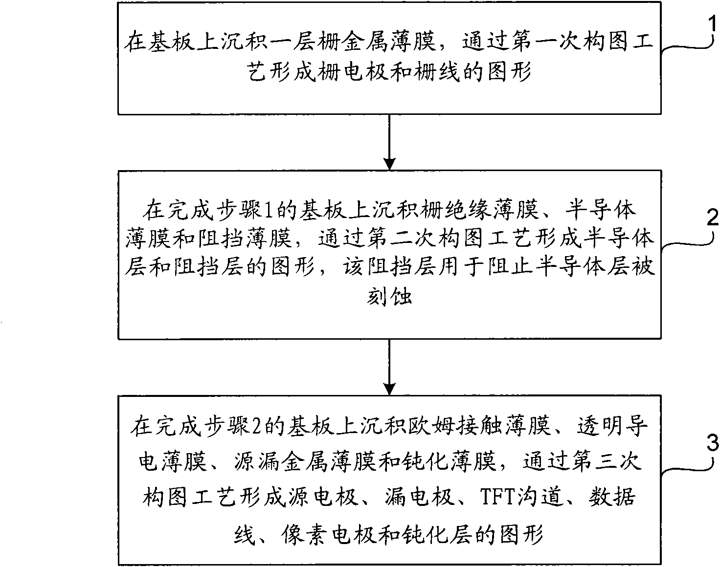
[0027] Such as figure 1 Shown is the flow chart of the TFT-LCD array substrate manufacturing method of the present invention, including:
[0028] Step 1, depositing a layer of gate metal thin film on the substrate, and forming the pattern of gate electrode and gate line through the first patterning process;
[0029] Step 2. Depositing a gate insulating film, a semiconductor film and a barrier film on the substrate completed in step 1, and forming a pattern of the semiconductor layer and the barrier layer through a second patterning process, the barrier layer is used to prevent the semiconductor layer from being etched;
[0030] Step 3. Deposit ohmic contact film, transparent conductive film, source-drain metal film and passivation film on the substrate after step 2, and form source electrode, drain electrode, channel, data line, pixel electrode and Graphics of the passivation layer.
[0031] The specific implementation process of each step is introduced in detail below.
[...
PUM
| Property | Measurement | Unit |
|---|---|---|
| Thickness | aaaaa | aaaaa |
| Thickness | aaaaa | aaaaa |
Abstract
Description
Claims
Application Information
PatSnap Eureka turns technology decisions into work you can execute. Powered by our Innovation Knowledge Graph, it runs expert workflows across engineering, life sciences, materials and intellectual property. Get your review-ready output in minutes.


