
Wide band radio-frequency low noise amplifier with single-ended input and differential output

A low-noise amplifier, differential output technology, used in differential amplifiers, DC-coupled DC amplifiers, amplifiers, etc., can solve the problem that the input impedance matching and low noise cannot be achieved, the amplifier cannot achieve broadband applications, and the realization of high integration is limited. problem, to achieve the effect of compact structure, improved dynamic range, and low power consumption of the circuit

Inactive Publication Date: 2010-07-14
南京广嘉微电子有限公司
View PDF2 Cites 46 Cited by
  • Summary
  • Abstract
  • Description
  • Claims
  • Application Information

AI Technical Summary

Problems solved by technology

The signals coming in from the antenna are often single-ended input, so it is necessary to realize the conversion from single-ended to differential. The traditional differential RF low-noise amplifier requires an additional single-turn dual (balun) module, and many designs use passive balance conversion. The device is connected before the RF low noise amplifier to realize the conversion from single-ended to differential, but this method will introduce additional loss and deteriorate the system noise performance
[0006] Although the prior art has solved some problems, there are still many deficiencies, such as: the invention patent CN02123628.3 of Li Yongming and others proposes a single-ended to differential radio frequency low noise amplifier with variable gain, and the radio frequency low noise amplifier Designed as a single-ended structure, placing the single-ended-to-differential balun after the RF low-noise amplifier has the advantage of reducing the extra noise introduced by the off-chip balun, and at the same time reduces the power compared to the fully differential RF low-noise amplifier. However, due to the introduction of a lot of inductance in the main amplifier circuit and the single-ended to differential circuit, it is not conducive to system integration. In addition, the amplifier cannot realize broadband applications; the invention patent of Uday Dasgupta et al. US 6,566,961B2 "Wide-band Single -ended todifferential Converter in CMOS technology" proposed a differential-to-broadband balun conversion circuit, although it has good phase and amplitude balance, but it cannot meet the requirements of input impedance matching and low noise; Fernando Azevedo et al's paper " AWideband CMOS LNA Integrated with Balun and Linear Digital GainControl", and the paper "A New GainControllable On-Chip Active Balun for 5GHz Direct Conversion Receiver" by Mallesh Rajashekharaiah et al. The structure of the low noise amplifier plus balun is similar to that of patent CN02123628.3 , are narrow-band amplifiers matched by a single frequency point, and the use of a large number of inductors also limits the realization of high integration, and the low-noise amplifier and balun are independently designed, so each consumes a lot of current; S.C.Blaakmeer et al. The active balun proposed in the paper "AnInductorless Wideband Balun-LNA in 65nm CMOS with balanced output" can achieve low noise and single-to-double at the same time, but the power consumption of this design is very large; and the bias circuit does not propose a reasonable solution , so that the balance of the differential output itself is greatly affected by the change of the bias voltage, and it cannot reasonably compensate the temperature and process deviation, so it only stays in the early stage of academic research and cannot meet the needs of product design.

Method used


Image

  • Wide band radio-frequency low noise amplifier with single-ended input and differential output
  • Wide band radio-frequency low noise amplifier with single-ended input and differential output
  • Wide band radio-frequency low noise amplifier with single-ended input and differential output

Examples


Embodiment 1

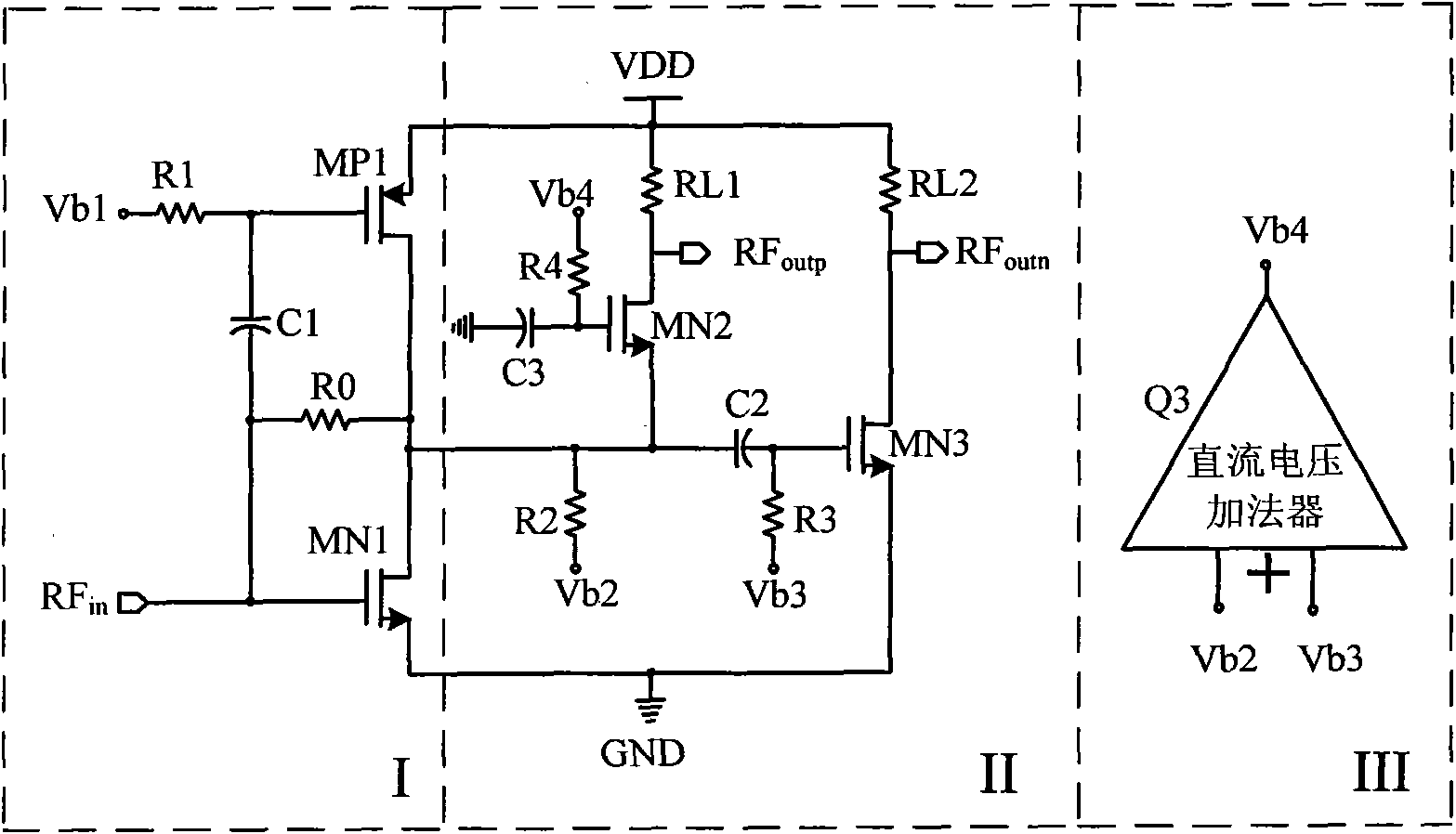
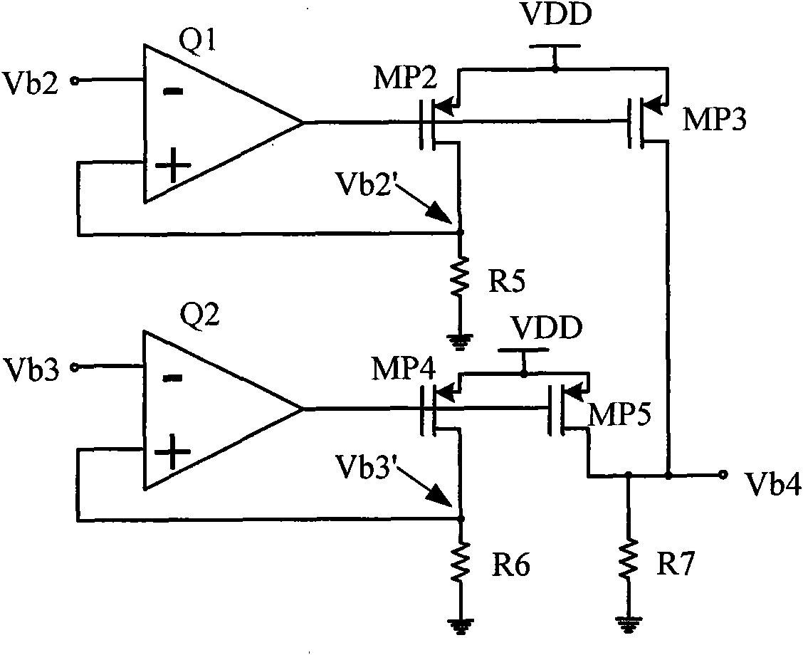
[0030] The broadband radio frequency low-noise amplifier of the single-ended input differential output that the present invention proposes, mainly comprises three parts: main amplifying circuit, such as figure 1 Shown in the dotted box I; single-ended to differential conversion active balun, such as figure 1 Shown in virtual box II; DC voltage operation circuit, such as figure 1 Shown in dashed box III.

[0031] The main amplifying circuit is mainly composed of main amplifying N-type transistor MN1 and auxiliary P-type amplifying transistor MP1, resistor RO, and capacitor C1. The connection relationship is: radio frequency signal RF in Input to the gate of the transistor MN1, the source of the transistor MN1 is grounded to GND, the drain of the transistor MN1 is connected to the drain of the transistor MP1, and at the same time connected to one end of the resistor RO; the other end of the resistor RO is connected to the gate of the transistor MN1, At the same time, it is con...


PUM


Abstract

The invention relates to a wide band radio-frequency low noise amplifier with single-ended input and differential output, belonging to the technical field of radio-frequency integrated circuits. The broadband radio-frequency low noise amplifier comprises a main amplifying circuit with the single-ended input, an active balun and an offset control circuit, wherein the active balun is connected with the main amplifying circuit and is converted from being single-ended to be differential; the main amplifying circuit mainly comprises an N-shaped transistor and a P-shaped transistor; and the active balun from being single-ended to be differential comprises a common-gate amplifying circuit and a common-source amplifying circuit. The low noise amplifier has very wide working frequency range, can cover the frequency range of a digital television from 50 MHz to 860 MHz and even wider, is suitable for wide bands and multi-mode multi-protocol communication system integration, and reduces the equipment cost. The invention can reduce the power consumption and the volume of the low noise amplifier, increase the gain, optimize the noise and enhance the linearity, also has simple structure, decreases off-chip elements, eliminates extra system noise generated by an off-chip balun, has extensive application potential in a wireless communication receiving system, and the like.

Description

technical field [0001] The invention belongs to the technical field of wireless communication, and relates to the amplifier structure design in radio frequency integrated circuit (RFIC) technology, specifically a wideband radio frequency low noise amplifier with single-end input and differential output. Background technique [0002] In recent years, with the rapid development of wireless communication technology, the corresponding product market has been continuously enriched, such as pagers, mobile phones, global positioning system (GPS), radio frequency identification (RFID), short-distance wireless communication and data transmission, digital TV (DVB) , wireless local area network (WLAN) and so on. These areas have higher and higher requirements for product performance, power consumption, volume and cost, which promotes the development of wireless transceiver modules in the direction of miniaturization, low power consumption and low cost, thus bringing great challenges to...

Claims


Application Information

Patent Timeline
IPC IPC(8): H03F3/193H03F3/45
CPCY02B60/50
Inventor 潘攀
Owner 南京广嘉微电子有限公司
Learn More