Supercharge Your Innovation With Domain-Expert AI Agents!

Complementary metal oxide semiconductor switch

A technology of oxide semiconductors and complementary metals, applied in semiconductor devices, semiconductor/solid-state device components, electronic switches, etc., can solve the problem of not maintaining the feedback signal point well, affecting the isolation of switches, and deviating from high-level feedback, etc. problem, achieve the effect of maintaining level, improving isolation and reducing signal distortion

Inactive Publication Date: 2010-07-21
BEIJING INSTITUTE OF TECHNOLOGYGY
View PDF0 Cites 1 Cited by
  • Summary
  • Abstract
  • Description
  • Claims
  • Application Information

AI Technical Summary

Problems solved by technology

But in a circuit structure with a cascaded feedback system, such as Figure 6B As shown, the feedback part is connected to the circuit by point XP through the control of switch p2 to form a feedback loop. When switches p1 and p2 are single heat sink switches, when p1 is open and p2 is closed, due to Figure 5B If the P pole of the PN junction diode shown in is connected to the high-level feedback (VREFP), the PN junction diode is forward-conducting, which seriously affects the isolation when the switch is turned off, so that the feedback signal point cannot be well maintained. level, resulting in an offset effect, resulting in severe signal distortion, and its output waveform is shown in Figure 7A shown
Depend on Figure 7A It can be seen that when the single heat sink switch p1 is closed and p2 is open, the output signal can completely follow the change of the input signal, but when the single heat sink switch p1 is open and p2 is closed, it is seriously affected by the cascade feedback system Deviates from high level feedback (VREFP), causing severe distortion of the signal

Method used


Image

  • Complementary metal oxide semiconductor switch
  • Complementary metal oxide semiconductor switch
  • Complementary metal oxide semiconductor switch

Examples


Embodiment Construction

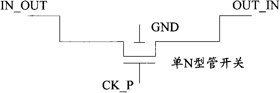
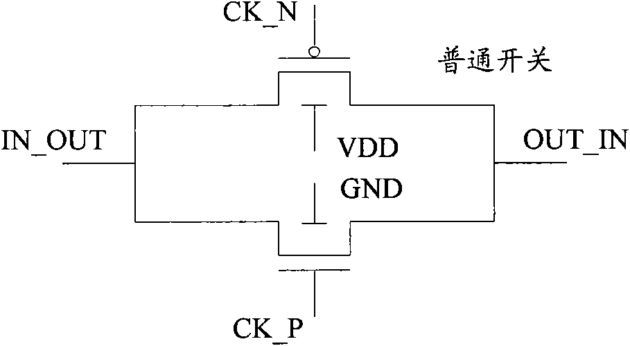
[0035] Aiming at the problem that the current single heat sink switch has a circuit structure with a cascaded feedback system, when the switch is turned off, the level of the feedback signal point cannot be well maintained, resulting in serious distortion of the signal. The present invention implements The example provides a CMOS switch, including two heat sink P-type tubes, wherein, the N-well of each P-type tube is connected to the source of the P-type tube, not connected to the power supply voltage (VDD), and the two The drains of the P-type tubes are connected to each other. When the CMOS switch (also known as a double heat sink switch) is turned off, due to the introduction of a PN junction diode that is opposite to the direction of the voltage drop, the N pole of the PN junction diode When connected to a high level, the PN junction diode is reversely cut off, thereby improving the isolation when the switch is turned off. Therefore, in a circuit structure with a cascaded f...


PUM


Abstract

The invention relates to the technical field of integrated circuits, in particular to a complementary metal oxide semiconductor (CMOS) switch which comprises a first thermal trap P-shaped pipe, a second thermal trap P-shaped pipe and an N-shaped pipe, wherein an N trap of the first thermal trap P-shaped pipe is connected with a source electrode; an N trap of the second thermal trap P-shaped pipe is connected with the source electrode, and the drain electrode of the second thermal trap P-shaped pipe is connected with the drain electrode of the first thermal trap P-shaped pipe; and the source electrode of the N-shaped pipe is connected with the source electrode of the first thermal trap P-shaped pipe, and the drain electrode of the N-shaped pipe is connected with the source electrode of the second thermal trap P-shaped pipe. When the CMOS switch is disconnected, because a PN junction diode with the direction opposite to the voltage drop direction is introduced, when the N electrode of the PN junction diode is connected with a high level, the PN junction diode is in a reverse cut-off state, and thus, the isolation performance of the switch during disconnection is improved. Therefore, in a circuit structure provided with a cascade feedback system, when the switch is disconnected, the level of a feedback signal point can be well maintained, and signal distortion is reduced.

Description

technical field [0001] The invention relates to the technical field of integrated circuits, in particular to a complementary metal oxide semiconductor (CMOS) switch. Background technique [0002] In an integrated circuit, the transmission of control signals through the on and off of switches is one of the main modes of operation of Complementary Metal Oxide Semiconductor (CMOS, Complementary Metal Oxide Semiconductor) devices. At present, switched capacitor (SC, Switched-Capacitor) circuits based on CMOS switches are widely used in signal filtering, analog signal processing, and high-frequency signal processing in data acquisition systems, such as amplifiers, oscillators, and balanced modulators. , analog multipliers, peak detectors, rectifiers, digital-to-analog (D / A) and analog-to-digital (A / D) converters, analog delays for video signals, and amplitude modulation (AM) / frequency modulation (FM) communication systems part of the circuit. It can be seen that the CMOS switch...

Claims


Application Information

Patent Timeline
Patent Type & Authority Applications(China)
IPC IPC(8): H03K17/687H01L27/092H01L23/522
Inventor 陈越洋王兴华仲顺安赵显利
Owner BEIJING INSTITUTE OF TECHNOLOGYGY
Features
  • R&D
  • Intellectual Property
  • Life Sciences
  • Materials
  • Tech Scout
  • Unparalleled Data Quality
  • Higher Quality Content
  • 60% Fewer Hallucinations
Learn More