Chiral sensor and preparation method thereof

A sensor and chirality technology, applied in the field of sensors, can solve the problem that the detection accuracy of chiral substances cannot meet the actual needs of enantiomer identification, and achieve simple device structure and principle, diverse and flexible materials, reduced volume and cost effect

Inactive Publication Date: 2010-07-28
SUZHOU INST OF NANO TECH & NANO BIONICS CHINESE ACEDEMY OF SCI
View PDF1 Cites 16 Cited by
  • Summary
  • Abstract
  • Description
  • Claims
  • Application Information

AI Technical Summary

Problems solved by technology

In addition to the use of enzymes for isomer-selective catalysis, the chiral selectors currently used in chiral sensors are mainly macrocyclic compounds and molecularly imprinted polymers. meet actual needs

Method used


Image

  • Chiral sensor and preparation method thereof
  • Chiral sensor and preparation method thereof
  • Chiral sensor and preparation method thereof

Examples


Embodiment 1

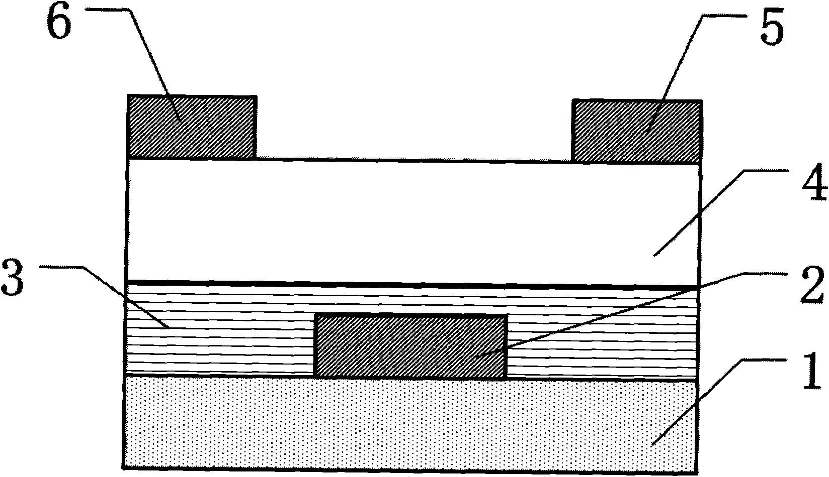
[0024] What is obtained by this preparation method is a bottom contact type chiral sensor:

[0025] Step 1: Sputtering or evaporating a layer of 10nm-500nm thick gate electrode 2 on the substrate 1. The gate electrode is composed of one or more of Ta, Ti, Cr, W, Mo, Au or Ag;

[0026] Step two, sputtering or evaporating a 150nm-500nm high dielectric constant gate insulating layer 3, the gate insulating layer 3 is made of SiO 2 , Ta 2 O 5 , Al 2 O 3 , TiO 2 , BZT or PZT one or two of them.

[0027] Step three, by vacuum thermal evaporation, spin coating, inkjet printing or screen printing a layer of 10nm-500nm thick active layer 4, the active layer 4 includes the following two different compositions (a), single chirality Organic semiconductors; (b) Chiral materials doped organic semiconductors.

[0028] Step 4: On the active layer 4, sputtering, inkjet printing or evaporating a layer of source electrode 5 and drain electrode 6 composed of one or two of Au, Ag, Ti, PEDOT:PSS, etc.

Embodiment 2

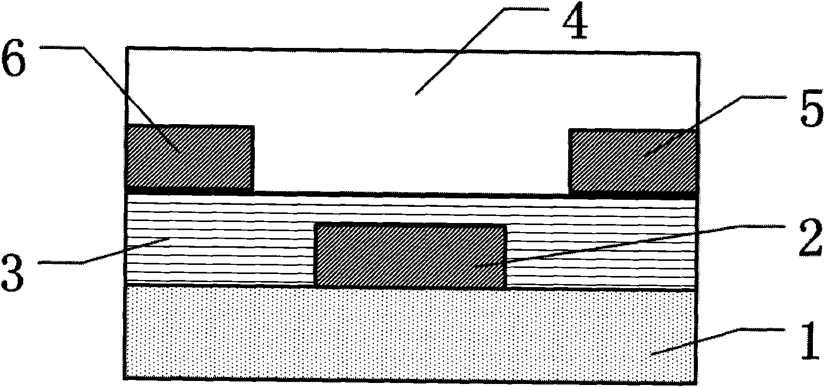
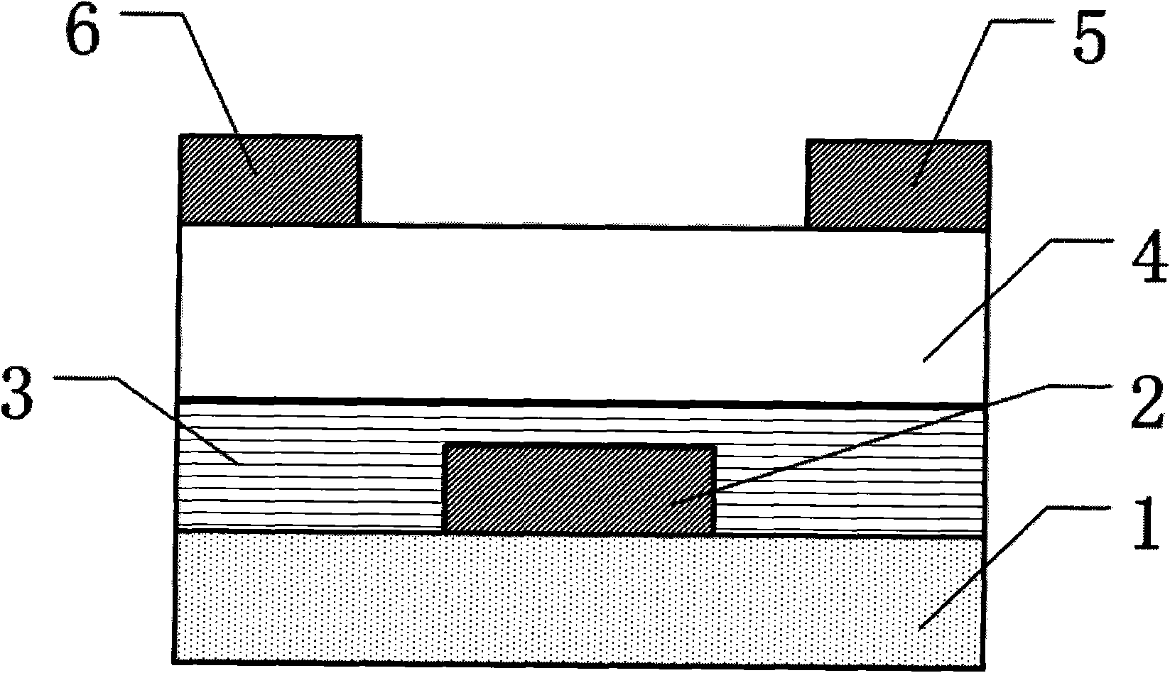
[0030] What is obtained by this preparation method is a top contact type chiral sensor:

[0031] Step 1: Sputtering or evaporating a layer of 10nm-500nm thick gate electrode 2 on the substrate 1. The gate electrode is composed of one or more of Ta, Ti, Cr, W, Mo, Au or Ag;

[0032] Step two, sputtering or evaporating a 150nm-500nm high dielectric constant gate insulating layer 3, the gate insulating layer 3 is made of SiO 2 , Ta 2 O 5 , Al 2 O 3 , TiO 2 , BZT or PZT one or two of them.

[0033] Step 3: On the gate insulating layer 3, sputtering, ink-jet printing or evaporating a layer of source electrode 5 and drain electrode 6 composed of one or two of Au, Ag, Ti, PEDOT:PSS, etc.

[0034] Step four, vacuum thermal evaporation, spin coating, ink-jet printing or screen printing on the gate insulating layer 3 and the source and drain electrodes is an active layer 4 with a thickness of 10nm-500nm, the composition of which can be selected as in the first embodiment.


PUM

PropertyMeasurementUnit
thicknessaaaaaaaaaa
thicknessaaaaaaaaaa

Abstract

The invention discloses a chiral sensor and a preparation method thereof. The chiral sensor provided with an organic field effect transistor as the basic structure thereof comprises a substrate, a gate insulation layer, an active layer, a gate electrode, a source electrode and a drain electrode, wherein the chiral sensor is characterized in that the active layer of the organic field effect transistor is made of organic semiconductor materials having the functions of chiral recognition and detection, more particularly, the component of the active layer can be a single chiral semiconductor material or alternatively an organic semiconductor material doped with a chiral material. By improving the materials of the active layer, the chiral sensor and the preparation method of the invention based on the organic field effect transistor can achieve the flexible detection of various chiral substances within a wide range and the identification of the corresponding isomers; and besides, the organic field effect transistor is small-sized, thus reducing the size and cost of detection components in application.

Description

Technical field [0001] The present invention relates to a sensor for chiral recognition research, in particular to a chiral sensor based on an organic field effect transistor structure and a preparation method thereof. The chiral sensor can change the performance of the field effect transistor device, and can be low-cost and Wide range and high sensitivity detection of chiral substances, involving materials, chemistry, organic optoelectronics and other interdisciplinary fields. Background technique [0002] With the application of chiral compounds in the fields of medicine, pesticides, perfumes, food additives, new materials, etc., people have attracted widespread attention. The synthesis, resolution and determination of enantiomeric purity of chiral compounds have become the frontiers of current chemistry. one. [0003] Chiral recognition research methods mainly include chiral chromatography (such as gas chromatography, liquid chromatography and capillary electrophoresis, etc.), ...

Claims


Application Information

Patent Timeline
Patent Type & Authority Applications(China)
IPC IPC(8): G01N27/414H01L51/05H01L51/40
Inventor 王凤霞王亦潘革波蒋春萍
Owner SUZHOU INST OF NANO TECH & NANO BIONICS CHINESE ACEDEMY OF SCI
Why Eureka
Try Eureka