

GaN-based vertical structure light-emitting diode and preparation method thereof
A technology of light-emitting diodes and vertical structures, applied in electrical components, circuits, semiconductor devices, etc., can solve problems such as increasing technical difficulty, and achieve the effects of improving electrical performance, simplifying manufacturing processes, and increasing surface electron concentration
- Summary
- Abstract
- Description
- Claims
- Application Information
AI Technical Summary
Problems solved by technology
Method used
Image

Examples
Embodiment 1
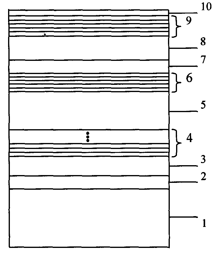
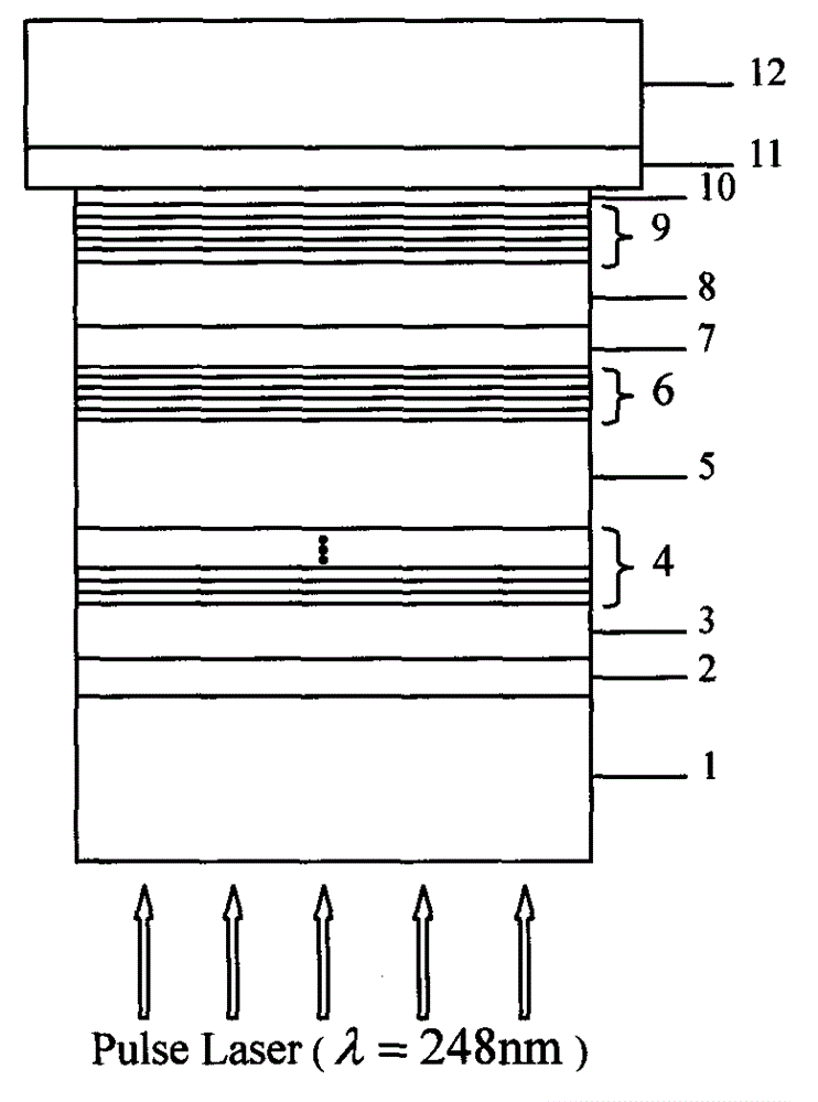
[0046] 1) Put the no-clean (0001) sapphire substrate into the reaction chamber, 2 Under the atmosphere, heat to 1050°C and bake for 20 minutes, cool down to 500°C to nitride the substrate for 150s, and the pressure of the reaction chamber is 50 Torr.
[0047] 2) Grow a GaN buffer layer with a thickness of 15nm at 500°C, the growth pressure is 200Torr, the flow rate of carrier gas is 10L / min, the flow rate of TMGa is 20μmol / min, NH 3 The flow rate is 80mol / min; then the temperature is raised to 1030°C and kept for 15min to recrystallize the GaN buffer layer.
[0048] 3) Grow the first silicon-doped GaN layer of 0.1 μm at 950 ° C, the growth pressure is 100 Torr, the flow rate of carrier gas is 5 L / min, the flow rate of TMGa is 80 μmol / min, NH 3 The flow rate is 120μmol / min, SiH 4 The flow rate is 0.2nmol / min.
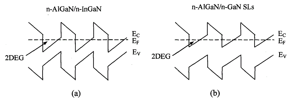
[0049] 4) Then grow the n-AlGaN / n-InGaN superlattice layer for 5 cycles by lowering the temperature, wherein the n-AlGaN layer growth temperature is 800°C, the growth...
Embodiment 2
[0057] 1) Put the no-clean (0001) sapphire substrate into the reaction chamber, 2 Under the atmosphere, heat to 1100°C and bake for 15 minutes, then lower the temperature to 900°C to nitride the substrate for 100s, and the pressure of the reaction chamber is 50 Torr.
[0058] 2) Grow a GaN buffer layer with a thickness of 25nm at 530°C, the growth pressure is 300Torr, the flow rate of carrier gas is 15L / min, the flow rate of TMGa is 50μmol / min, NH 3 The flow rate is 100mol / min; then the temperature is raised to 1040° C. and kept for 10 minutes to recrystallize the GaN buffer layer.
[0059] 3) Grow the first silicon-doped GaN layer of 0.2 μm at 1000 ° C, the growth pressure is 150 Torr, the flow rate of carrier gas is 15 L / min, the flow rate of TMGa is 300 μmol / min, NH 3 The flow rate is 300μmol / min, SiH 4 The flow rate is 1 nmol / min.
[0060] 4) Then grow the n-AlGaN / n-InGaN superlattice layer for 6 cycles by lowering the temperature, wherein the growth temperature of the ...
Embodiment 3
[0068] 1) Put the no-clean (0001) sapphire substrate into the reaction chamber, 2 Under the atmosphere, heat to 1150°C and bake for 10 minutes, then lower the temperature to 700°C to nitride the substrate for 120s, and the pressure of the reaction chamber is 50 Torr.
[0069] 2) Grow a GaN buffer layer with a thickness of 20nm at 550°C, the growth pressure is 500Torr, the flow rate of carrier gas is 20L / min, the flow rate of TMGa is 100μmol / min, NH 3 The flow rate is 110mol / min; then the temperature is raised to 1040° C. and kept for 10 minutes to recrystallize the GaN buffer layer.
[0070] 3) Grow the first silicon-doped GaN layer of 0.15 μm at 1050 ° C, the growth pressure is 200 Torr, the flow rate of carrier gas is 10 L / min, the flow rate of TMGa is 200 μmol / min, NH 3 The flow rate is 400μmol / min, SiH 4 The flow rate is 1.5 nmol / min.
[0071] 4) Then grow 8 cycles of n-AlGaN / n-GaN superlattice layer, where the n-AlGaN layer growth temperature is 1030°C, the growth thic...
PUM
| Property | Measurement | Unit |
|---|---|---|
| Resistivity | aaaaa | aaaaa |
| Thickness | aaaaa | aaaaa |
| Thickness | aaaaa | aaaaa |
Abstract
Description
Claims
Application Information