Eureka AIR delivers breakthrough ideas for toughest innovation challenges, trusted by R&D personnel around the world.

Gallium nitride transistor epitaxial structure capable of improving surface electron concentration and preparation method thereof

A technology of electron concentration and epitaxial structure, which is applied in semiconductor/solid-state device manufacturing, circuits, electrical components, etc., can solve the problem that the development has a great impact, the GaN thick film lattice matching and stress matching effects are limited, and the high quality of GaN thin films is restricted. Problems such as low stress state, to achieve high peak strength, improve crystal quality, and relieve stress

Pending Publication Date: 2022-02-25
JIANGSU INST OF ADVANCED SEMICON CO LTD
View PDF0 Cites 1 Cited by
  • Summary
  • Abstract
  • Description
  • Claims
  • Application Information

AI Technical Summary

Problems solved by technology

However, this type of material has limited lattice matching and stress matching effects on subsequent GaN thick films, which restricts the growth of high-quality and low-stress GaN films in the later stage, and has a great impact on the development of high-performance GaN devices that require thicker films. Especially two-dimensional devices with high interface requirements that use polarization effects to generate high-concentration electrons and high mobility

Method used


Image

  • Gallium nitride transistor epitaxial structure capable of improving surface electron concentration and preparation method thereof
  • Gallium nitride transistor epitaxial structure capable of improving surface electron concentration and preparation method thereof
  • Gallium nitride transistor epitaxial structure capable of improving surface electron concentration and preparation method thereof

Examples


Embodiment 1

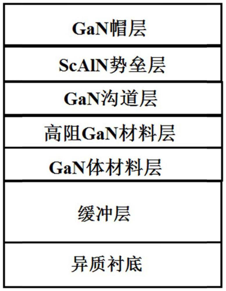
[0015] A method for preparing epitaxial structures of gallium nitride transistors with increased surface electron concentration, used for preparing such as figure 1 The epitaxial structure of the gallium nitride transistor shown is arranged in sequence on the heterogeneous substrate: a buffer layer composed of a multi-layer ScAlN layer with a gradient composition, a GaN bulk material layer, a high-resistance GaN material layer, and a GaN channel Layer, ScAlN barrier layer and GaN cap layer, its preparation method comprises the following steps:

[0016] Step 1: Depositing a multi-layer ScAlN buffer layer with a gradient composition on the heterogeneous substrate, the total thickness is 20-50nm, and the number of layers is 2-10 layers;

[0017] Step 2: performing high-temperature recrystallization on the buffer layer to form a nucleation center, and growing a GaN bulk material layer on the buffer layer with a thickness of about 1-2 μm;

[0018] Step 3: growing an Fe-doped or C-...

Embodiment 2

[0024] A method for preparing a gallium nitride transistor epitaxial structure for increasing surface electron concentration, the growth of which includes the following steps:

[0025] Step 1: Under the reaction chamber pressure of 200torr and temperature of 700°C, 10nm ScAlN with 10% Sc composition, 10nm ScAlN with 15% Sc composition and 10nm Sc composition with 20% ScAlN;

[0026] Step 2: Increase the pressure to 500torr, temperature 1070°C, and hold the temperature for 5 minutes, then lower the temperature to 1040°C, pass through TMGa for three-dimensional growth, with a thickness of about 500nm, then reduce the pressure to 200torr, raise the temperature to 1090°C, and carry out Merge growth from 3D to 2D to form a GaN bulk material layer as the underlying material layer;

[0027] Step 3: Access to C 3 h 8 Carry out C doping of GaN material to form a high-resistance GaN material growth of about 4 μm;

[0028] Step 4: Close C 3 h 8 , to grow a non-doped GaN channel lay...


PUM

PropertyMeasurementUnit
thicknessaaaaaaaaaa
thicknessaaaaaaaaaa
thicknessaaaaaaaaaa

Abstract

The invention discloses a gallium nitride transistor epitaxial structure capable of improving surface electron concentration and a preparation method thereof. The method comprises the following steps of sequentially depositing a plurality of ScAlN layers with gradually-changed components on a heterogeneous substrate as a buffer layer, carrying out the high-temperature recrystallization of the buffer layer, forming a nucleation center, carrying out the three-dimensional growth of a GaN material, and carrying out the combined growth of three-dimensional to two-dimensional growth, forming abottom layer structure and growing epitaxial structures such as a high-resistance GaN material, a GaN channel layer, an ScAlN barrier layer and a GaN cap layer on the bottom layer structure. The method has the beneficial effects that the bottom layer of the sample adopts the lattice-matched ScAlN buffer layer for transition, so that the GaN body material layer is higher in crystal quality and smoother in surface; meanwhile, before the ScAlN material barrier layer is grown, the buffer layer at the bottom layer can perform secondary stress release, so that the whole epitaxial structure is in a zero stress state, the interface quality among the layers is improved, and the transistor has higher surface electron concentration under the GaN / ScAlN polarization effect and is suitable for being applied to acousto-optic devices.

Description

technical field [0001] The invention relates to the field of semiconductor material technology, in particular to an epitaxial structure of a high surface electron concentration transistor and a preparation method thereof. Background technique [0002] With the rapid development of third-generation semiconductor materials and devices represented by GaN and SiC, the demand for high-quality GaN thin film materials is becoming more and more urgent. Because the GaN single crystal heterogeneous substrate is relatively expensive, the current mainstream GaN thin film materials are all obtained by heteroepitaxy method on the heterogeneous substrate. The dislocation density of the crystal quality of this thin film material is between 10 8 cm -2 There is still a lot of room for improvement. At present, the mainstream method of heteroepitaxy is the two-step growth method, and (Al)GaN material is selected as the buffer layer, which is used as the transition between the heterogeneous su...

Claims


Application Information

Patent Timeline
Patent Type & Authority Applications(China)
IPC IPC(8): H01L21/20H01L21/335H01L29/20H01L29/207H01L29/778
CPCH01L21/0242H01L21/02458H01L21/0254H01L21/0257H01L29/7787H01L29/66462H01L29/2003H01L29/207
Inventor 王国斌刘宗亮
Owner JIANGSU INST OF ADVANCED SEMICON CO LTD
Why Eureka
Eureka Blog
Learn More