Eureka AIR delivers breakthrough ideas for toughest innovation challenges, trusted by R&D personnel around the world.

Preparation method and application of transparent electrode of ultraviolet light-emitting diode

A technology of light-emitting diodes and transparent electrodes, applied in chemical instruments and methods, circuits, electrical components, etc., can solve the problems of low specific contact resistance of transparent conductive films, achieve low forward operating voltage, promote application, and high light extraction efficiency Effect

Active Publication Date: 2018-02-16
SUN YAT SEN UNIV
View PDF2 Cites 2 Cited by
  • Summary
  • Abstract
  • Description
  • Claims
  • Application Information

AI Technical Summary

Problems solved by technology

[0005] Transparent electrodes prepared by conventional methods generally use a single growth condition, and the prepared film has high conductivity and transmittance; however, the transparent conductive film prepared under this condition may not necessarily achieve a low specific contact resistance with LEDs.

Method used


Image

  • Preparation method and application of transparent electrode of ultraviolet light-emitting diode
  • Preparation method and application of transparent electrode of ultraviolet light-emitting diode
  • Preparation method and application of transparent electrode of ultraviolet light-emitting diode

Examples


Embodiment 1

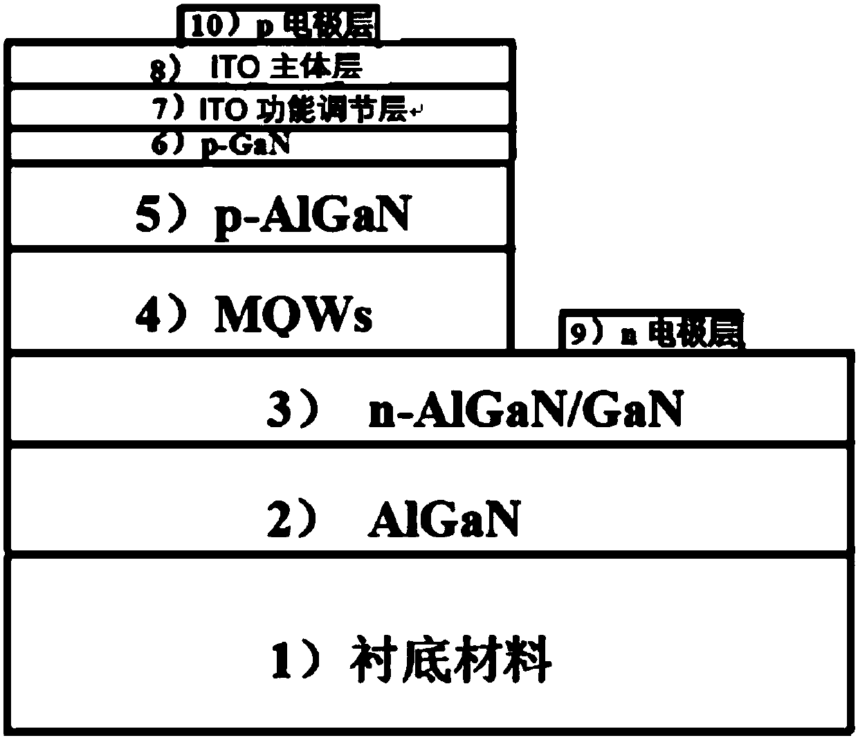
[0038] Using the existing MOCVD equipment, using organometallic trimethyl indium as the indium source, organometallic tetrakis (dimethylamino) tin source, oxygen with a purity of 99.9999% as the oxygen source, argon as the carrier gas and growth protective atmosphere, in the epitaxial wafer A functional adjustment layer of pre-applied organometallic In source is grown on the ultraviolet 365nm LED, and then a layer of ITO film is deposited as the main layer.

[0039] The preparation method of the function adjustment layer and the main body layer is as follows:

[0040] 1. Pretreatment before growing the substrate: Using 365nm UV LED epitaxial wafer as the substrate material, the surface of the substrate material is cleaned with organic and inorganic acid and alkali to prevent contact with air and put it into the MOCVD reaction chamber as soon as possible.

[0041] 2. Growth of the functional adjustment layer: the growth temperature is controlled at 530° C., the pressure in the ...

Embodiment 2

[0046] Using the existing MOCVD equipment, using organometallic trimethyl indium as the indium source, organometallic tetrakis (dimethylamino) tin source, oxygen with a purity of 99.9999% as the oxygen source, argon as the carrier gas and growth protective atmosphere, in the epitaxial wafer A layer of pre-spreading organometallic Sn function adjustment layer is grown on the ultraviolet 365nm LED, and then a layer of ITO film is deposited as the main layer.

[0047] The preparation method of the function adjustment and the main body layer is as follows:

[0048] 1. Pretreatment before growing the substrate: Using 365nm UV LED epitaxial wafer as the substrate material, the surface of the substrate material is cleaned with organic and inorganic acid and alkali to prevent contact with air and put it into the MOCVD reaction chamber as soon as possible.

[0049] 2. Growth of functional adjustment layer: the growth temperature is controlled at 530°C, the pressure of the reaction cham...


PUM


Abstract

The invention discloses a metal organic chemical vapor deposition (MOCVD) preparation method a transparent electrode used for an ultraviolet LED. The preparation method is characterized in that a functional adjusting layer is firstly grown in situ before a deposited and doped indium tin oxide (ITO) serves as a main body layer. The invention also discloses how to grow the functional adjusting layerand the main body layer in situ, the functional adjusting layer and the main body layer are grown in sequence on the surface of an ultraviolet LED epitaxial wafer as a growth substrate material. Themethod comprises the following steps: growing a substrate for pretreatment; introducing one of an indium source and a tin source or a mixed source of the indium source and the tin source into the surface of the nitride-based ultraviolet LED epitaxial water to form the functional adjusting layer; and introducing an indium source, a tin source and an oxygen source onto the functional adjusting layerto grow an ITO film so as to form the main body layer. The ITO transparent conducting film provided by the invention applied onto the nitride-based ultraviolet LED device has the advantages of low positive working voltage, extremely high reliability and efficient light extraction efficiency, and the application of the ultraviolet photoelectric device can be greatly promoted.

Description

technical field [0001] The invention relates to the technical field of semiconductor materials and semiconductor optoelectronic devices, in particular to a method for preparing a transparent electrode of an ultraviolet light-emitting diode and its application. Background technique [0002] Materials such as nickel-gold alloy (Ni / Au), zinc oxide-based transparent electrodes, and indium tin oxides (Indium Tin Oxides, ITO) are mainly used for the transparent electrode films of nitride-based light-emitting diodes (LEDs). [0003] Transparent conductive films have high transmittance and low resistivity in the visible light range (400nm-760nm), and are widely used in flat panel displays, solar cells, light-emitting devices, photodetectors and other fields, with broad application prospects. In recent years, photoelectric devices in the ultraviolet band have developed rapidly, and when used as transparent electrodes for ultraviolet LEDs, transparent conductive films are required to ...

Claims


Application Information

Patent Timeline
IPC IPC(8): H01L33/42C30B25/02
CPCC30B25/02H01L33/42H01L2933/0016
Inventor 王钢陈梓敏涂文斌卓毅
Owner SUN YAT SEN UNIV
Why Eureka
Eureka Blog
Learn More