Nanoscale size structure measuring method and device

A measurement method, nano-scale technology, applied in the direction of measuring devices, optical devices, instruments, etc., can solve the problems of inability to obtain clear imaging, unable to meet the requirements of accurate measurement of key dimensions of nano-scale structures, and achieve rapid geometric feature parameters, Promotes the effect of expanding applications and broad application prospects

Active Publication Date: 2010-08-11
HUAZHONG UNIV OF SCI & TECH
View PDF6 Cites 13 Cited by
  • Summary
  • Abstract
  • Description
  • Claims
  • Application Information

AI Technical Summary

Problems solved by technology

When the critical dimensions in nanomanufacturing reach the sub-wavelength nanometer level, traditional optical microscopes cannot obtain clear

Method used


Image

  • Nanoscale size structure measuring method and device
  • Nanoscale size structure measuring method and device
  • Nanoscale size structure measuring method and device

Examples


Embodiment Construction

[0022] Below in conjunction with accompanying drawing and example the principle of the inventive method and working process are described in further detail:

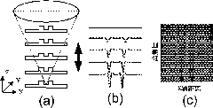
[0023] (1) After the white light beam is filtered and polarized, it is projected vertically onto the surface of the sample containing nanoscale structures, and the wavelength of the linearly polarized beam projected onto the surface of the sample is 400-600nm.

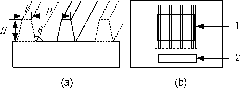
[0024] Taking the measurement process of the isolated line array structure as an example, the isolated line array structure is as follows figure 1 As shown in (a), the geometry parameters of the nanoscale structure to be measured include line width D, period P, depth H and side wall angle θ.

[0025] (2) The projected beam is reflected by the surface of the sample, and the reflected signal is received by a charge-coupled device (CCD) placed on the conjugate surface of the sample, and the microscopic imaging map of the nanoscale structure is calculated.

[0026] ...


PUM


Abstract

The invention discloses a nanoscale size structure measuring method and a device, which can simultaneously measure parameters, such as nanoscale size structure width, depth, side corner and the like. The method of the invention comprises the following steps: vertically projecting a white light beam to the surface of a sample workpiece with a nanoscale size structure after filtering and polarizing; collecting the surface reflected signal of the sample workpiece; calculating to obtain a nanoscale size structure microscope imaging picture; matching a measured outoffocus scanning imaging allocation plan with a theory outoffocus scanning imaging allocation plan; and extracting to obtain the geometric parameter value of the nanoscale size structure is to be measured. The nanoscale size structure measuring device provided by the invention can provide a non-contact, non-destructive, low-cost and quick measuring means for various typical nanoscale size structures, such as isolated line array structure and intensive line array structure to which the lot sizing manufacturing technology relates, and the lot sizing manufacturing technology comprises the nanometer manufacturing technology, such as traditional photoetching, nano-imprint and the like based on imaging transfer.

Description

technical field [0001] The invention belongs to nanometer manufacturing measurement technology, and specifically relates to a method and device for measuring key dimensions of nanometer-scale structures. Measurement of depth, side wall angle, and overlay accuracy of overlay graphics marks. Background technique [0002] Nanofabrication refers to the manufacturing technology whose characteristic size is on the order of nanometers. In recent years, with the intersection and integration of mechanics, physics, chemistry, biology, materials science, information science and other related disciplines, several new nano-manufacturing methods and new processes based on the principles of physics, chemistry and even biology have emerged, such as Bottom-up nano-scale structure growth, processing, modification, assembly and other nano-manufacturing technologies. At the same time, the traditional microelectronic integrated circuit (IC, Integrated Circuit) and microelectromechanical system...

Claims


Application Information

Patent Timeline
IPC IPC(8): G01B11/02G01B11/24G01B9/04
Inventor 刘世元张传维史铁林陈修国
Owner HUAZHONG UNIV OF SCI & TECH
Why Eureka
Try Eureka